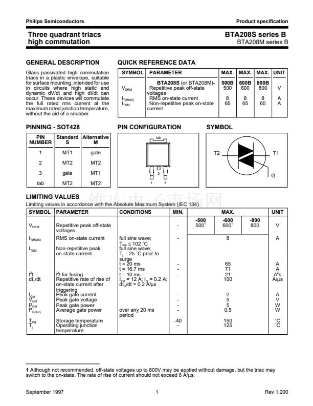
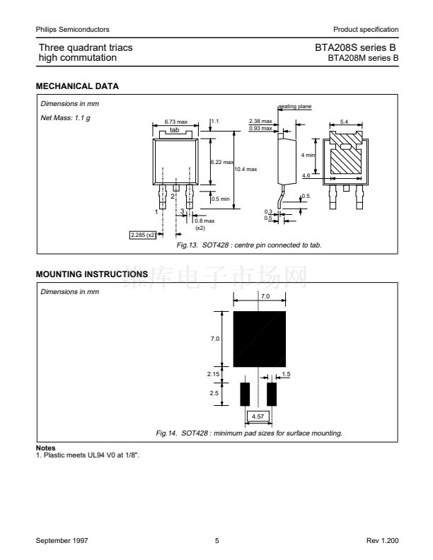
Philips Semiconductors
Product specification
Three quadrant triacs
high commutation
THERMAL RESISTANCES
SYMBOL
R
th j-mb
R
th j-a
PARAMETER
CONDITIONS
BTA208S series B
BTA208M series B
MIN.
-
-
-
TYP.
-
-
75
MAX.
2.0
2.4
-
UNIT
K/W
K/W
K/W
Thermal resistance
full cycle
junction to mounting base half cycle
Thermal resistance
pcb (FR4) mounted; footprint as in Fig.14
junction to ambient
STATIC CHARACTERISTICS
T
j
= 25 藲C unless otherwise stated
SYMBOL
I
GT
PARAMETER
Gate trigger current
2
CONDITIONS
V
D
= 12 V; I
T
= 0.1 A
T2+ G+
T2+ G-
T2- G-
T2+ G+
T2+ G-
T2- G-
MIN.
2
2
2
-
-
-
-
-
-
0.25
-
TYP.
18
21
34
31
34
30
31
1.3
0.7
0.4
0.1
MAX.
50
50
50
60
90
60
60
1.65
1.5
-
0.5
UNIT
mA
mA
mA
mA
mA
mA
mA
V
V
V
mA
I
L
Latching current
V
D
= 12 V; I
GT
= 0.1 A
I
H
V
T
V
GT
I
D
Holding current
On-state voltage
Gate trigger voltage
Off-state leakage current
V
D
= 12 V; I
GT
= 0.1 A
I
T
= 10 A
V
D
= 12 V; I
T
= 0.1 A
V
D
= 400 V; I
T
= 0.1 A; T
j
= 125 藲C
V
D
= V
DRM(max)
; T
j
= 125 藲C
DYNAMIC CHARACTERISTICS
T
j
= 25 藲C unless otherwise stated
SYMBOL
dV
D
/dt
dI
com
/dt
t
gt
PARAMETER
Critical rate of rise of
off-state voltage
Critical rate of change of
commutating current
Gate controlled turn-on
time
CONDITIONS
V
DM
= 67% V
DRM(max)
; T
j
= 125 藲C;
exponential waveform; gate open circuit
V
DM
= 400 V; T
j
= 125 藲C; I
T(RMS)
= 8 A;
without snubber; gate open circuit
I
TM
= 12 A; V
D
= V
DRM(max)
; I
G
= 0.1 A;
dI
G
/dt = 5 A/碌s
MIN.
1000
-
-
TYP.
4000
14
2
MAX.
-
-
-
UNIT
V/碌s
A/ms
碌s
2
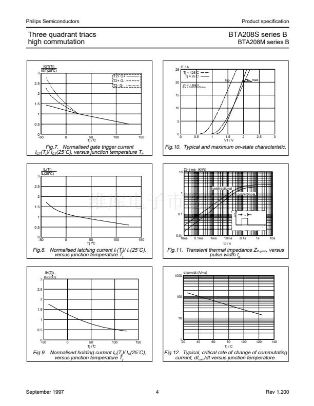
Device does not trigger in the T2-, G+ quadrant.
September 1997
2
Rev 1.200


 1
1
 2
2
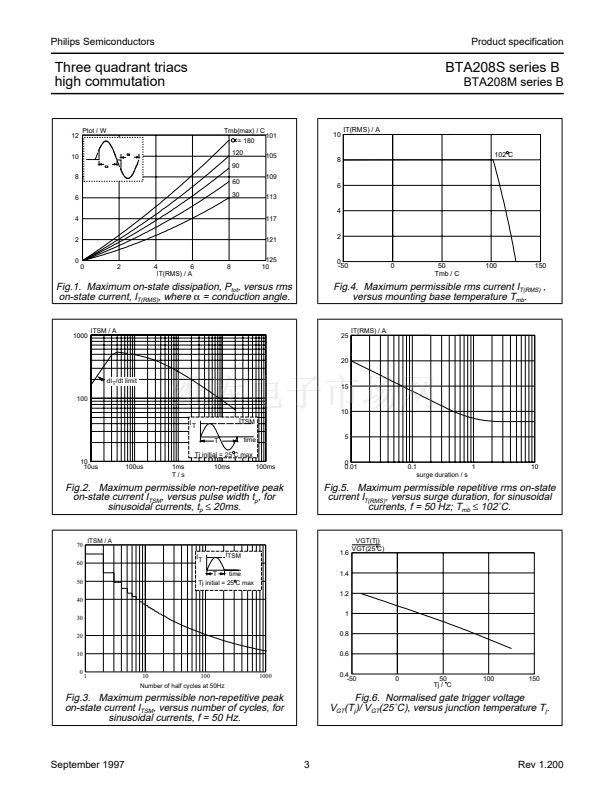 3
3
 4
4
 5
5
 6
6
 7
7
