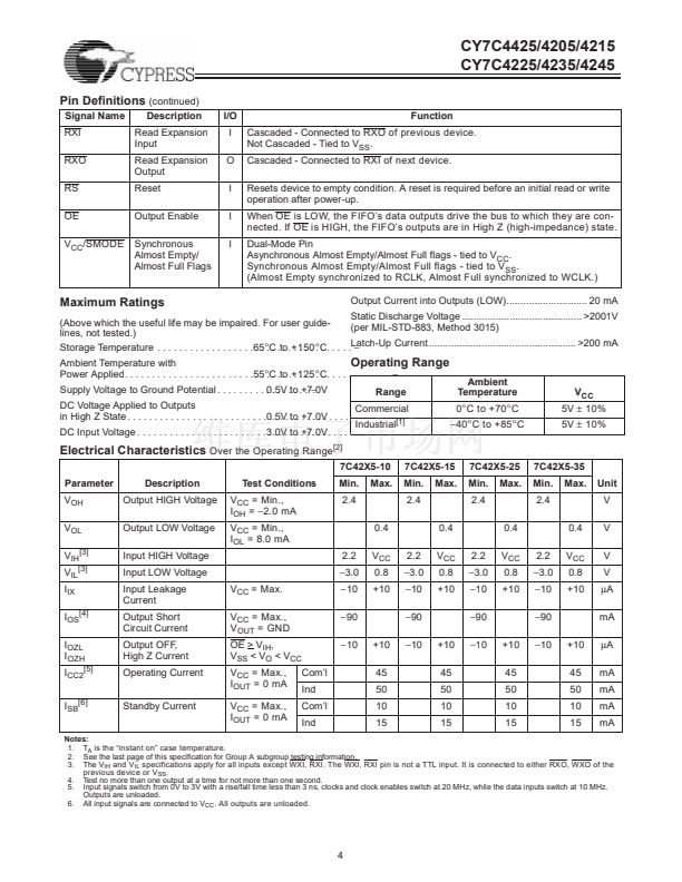
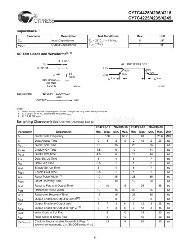
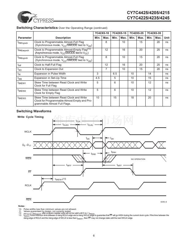
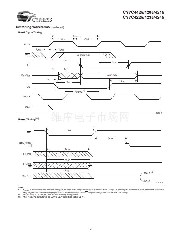
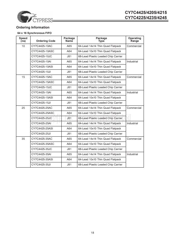
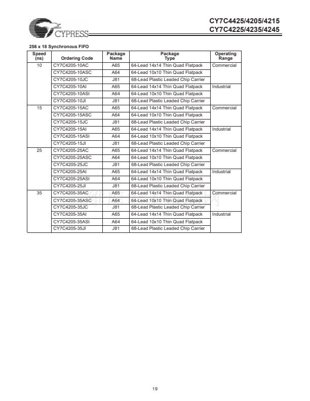
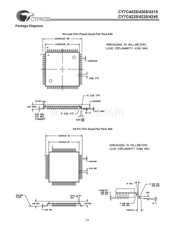
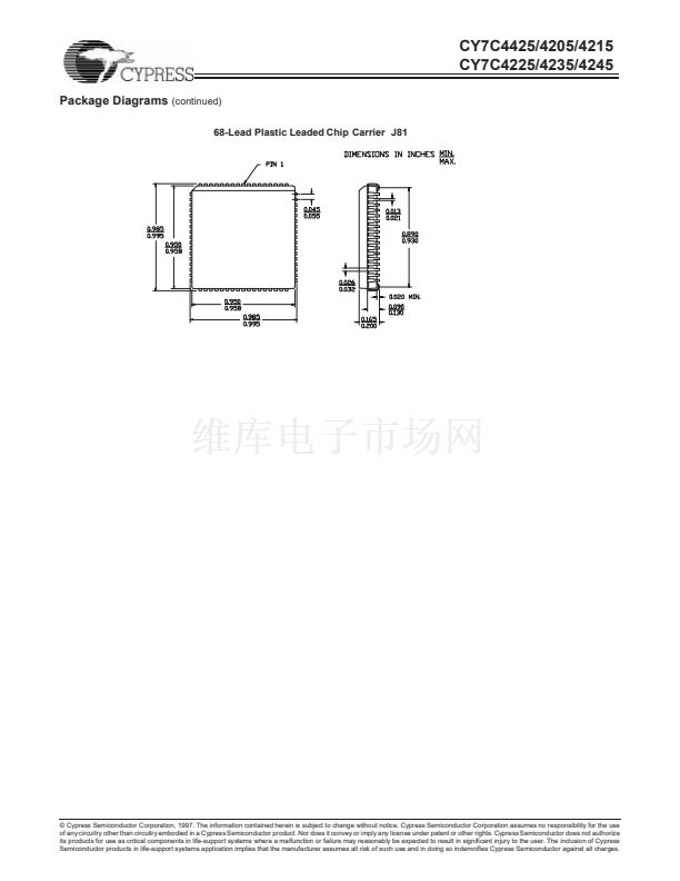
CY7C4425/4205/4215
CY7C4225/4235/4245
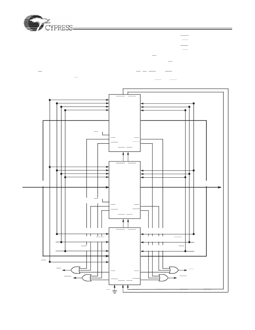
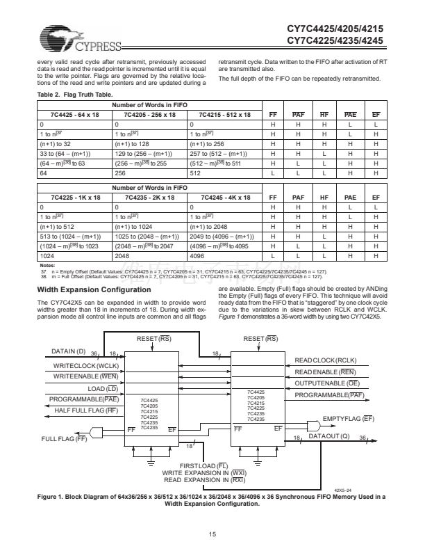
Depth Expansion Configuration
(with Programmable Flags)
The CY7C42X5 can easily be adapted to applications requir-
ing more than 64/256/512/1024/2048/4096 words of buffering.
Figure 2
shows Depth Expansion using three CY7C42X5s. Maxi-
mum depth is limited only by signal loading. Follow these steps:
1. The first device must be designated by grounding the First
Load (FL) control input.
2. All other devices must have FL in the HIGH state.
3. The Write Expansion Out (WXO) pin of each device must be
tied to the Write Expansion In (WXI) pin of the next device.
4. The Read Expansion Out (RXO) pin of each device must be
tied to the Read Expansion In (RXI) pin of the next device.
5. All Load (LD) pins are tied together.
6. The Half-Full Flag (HF) is not available in the Depth Expansion
Configuration.
7. EF, FF, PAE, and PAF are created with composite flags by
ORing together these respective flags for monitoring. The
composite PAE and PAF flags are not precise.
WXO RXO
7C4425
7C4205
7C4215
7C4225
7C4235
7C4235
FF
EF
PAE
PAF
WXI RXI
V
CC
FIRSTLOAD (FL)
WXO RXO
7C4425
7C4205
7C4215
7C4225
7C4235
7C4235
FF
EF
PAE
PAF
WXI RXI
DATAIN (D)
V
CC
FIRSTLOAD (FL)
DATAOUT (Q)
WRITECLOCK (WCLK)
WRITE ENABLE (WEN)
RESET(RS)
WXO RXO
7C4425
7C4205
7C4215
7C4225
7C4235
7C4235
FF
EF
READ CLOCK (RCLK)
READ ENABLE (REN)
OUTPUT ENABLE (OE)
LOAD (LD)
FF
PAF
EF
PAE
42X5鈥?3
PAFWXI RXIPAE
FIRSTLOAD (FL)
Figure 2. Block Diagram of 192 x 18/768 x 18/1536 x 18/3072 x 18/12288 x 18 Synchronous FIFO Memory
with Programmable Flags used in Depth Expansion Configuration.
16


 1
1
 2
2
 3
3
 4
4
 5
5
 6
6
 7
7
 8
8
 9
9
 10
10
 11
11
 12
12
 13
13
 14
14
 15
15
 16
16
 17
17
 18
18
 19
19
 20
20
 21
21
 22
22
 23
23
 24
24
 25
25
 26
26
