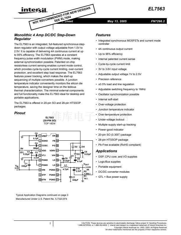
EL7563
Absolute Maximum Ratings
(T
A
= 25掳C)
Supply Voltage between V
IN
or V
DD
and GND . . . . . . . . . . . . +4.5V
V
LX
Voltage . . . . . . . . . . . . . . . . . . . . . . . . . . . . . . . . . . . . V
IN
+0.3V
Input Voltage . . . . . . . . . . . . . . . . . . . . . . . . GND -0.3V, V
DD
+0.3V
V
HI
Voltage . . . . . . . . . . . . . . . . . . . . . . . . . . . GND -0.3V, V
LX
+6V
Storage Temperature . . . . . . . . . . . . . . . . . . . . . . . .-65掳C to +150掳C
Operating Ambient Temperature . . . . . . . . . . . . . . . .-40掳C to +85掳C
Operating Junction Temperature . . . . . . . . . . . . . . . . . . . . . . +135掳C
CAUTION: Stresses above those listed in 鈥淎bsolute Maximum Ratings鈥?may cause permanent damage to the device. This is a stress only rating and operation of the
device at these or any other conditions above those indicated in the operational sections of this specification is not implied.
IMPORTANT NOTE: All parameters having Min/Max specifications are guaranteed. Typical values are for information purposes only. Unless otherwise noted, all tests
are at the specified temperature and are pulsed tests, therefore: T
J
= T
C
= T
A
DC Electrical Specifications
PARAMETER
V
REF
V
REFTC
V
REFLOAD
V
RAMP
I
OSC_CHG
I
OSC_DIS
I
VDD
+V
DRV
I
VDD_OFF
V
DD_OFF
V
DD_ON
T
OT
T
HYS
I
LEAK
I
LMAX
R
DSON
R
DSONTC
I
STP
I
STN
V
PGP
V
PGN
V
PG_HI
V
PG_LO
V
OVP
V
FB
V
FB_LINE
V
FB_LOAD
V
FB_TC
I
FB
V
EN_HI
V
EN_LO
I
EN
V
DD
= V
IN
= 3.3V, T
A
= T
J
= 25掳C, C
OSC
= 390pF, unless otherwise specified.
CONDITIONS
MIN
1.24
TYP
1.26
50
0 < I
REF
< 50碌A
-1
1.15
0.1V < V
OSC
< 1.25V
0.1V < V
OSC
< 1.25V
V
EN
= 2.7V, F
OSC
= 120kHz
EN = 0
2.4
2.6
135
20
EN = 0, L
X
= 3.3V (low FET), L
X
= 0V
(high FET)
5
Wafer level test only
30
0.2
V
STP
= V
IN
/2
V
STN
= V
IN
/2
With respect to target output voltage
With respect to target output voltage
I
PG
= 1mA
I
PG
= -1mA
10
I
LOAD
= 0A
V
IN
= 3.3V,
鈭哣
IN
= 10%, I
LOAD
= 0A
0.5A < I
LOAD
< 4A
-40掳C < T
A
< 85掳C, I
LOAD
= 2A
V
FB
= 0V
0.977
0.992
0.5
0.5
卤1
100
200
2.7
1
V
EN
= 0
-4
-2.5
1.007
6
-16
2.7
0.5
-4
2.5
2.5
4
16
-6
60
10
2
200
8
5.5
1
6.5
1.5
2.65
2.95
MAX
1.28
UNIT
V
ppm/掳C
%
V
碌A
mA
mA
mA
V
V
掳C
掳C
碌A
A
m鈩?/div>
m鈩?掳C
碌A
碌A
%
%
V
V
%
V
%
%
%
nA
V
V
碌A
DESCRIPTION
Reference Accuracy
Reference Temperature Coefficient
Reference Load Regulation
Oscillator Ramp Amplitude
Oscillator Charge Current
Oscillator Discharge Current
V
DD
+V
DRV
Supply Current
V
DD
Standby Current
V
DD
for Shutdown
V
DD
for Startup
Over Temperature Threshold
Over Temperature Hysteresis
Internal FET Leakage Current
Peak Current Limit
FET On Resistance
R
DSON
Tempco
Auxiliary Supply Tracking Positive Input
Pull Down Current
Auxiliary Supply Tracking Negative Input
Pull Up Current
Positive Power Good Threshold
Negative Power Good Threshold
Power Good Drive High
Power Good Drive Low
Over Voltage Protection
Output Initial Accuracy
Output Line Regulation
Output Load Regulation
Output Temperature Stability
Feedback Input Pull Up Current
EN Input High Level
EN Input Low Level
Enable Pull Up Current
3
FN7296.2
May 13, 2005


 1
1
 2
2
 3
3
 4
4
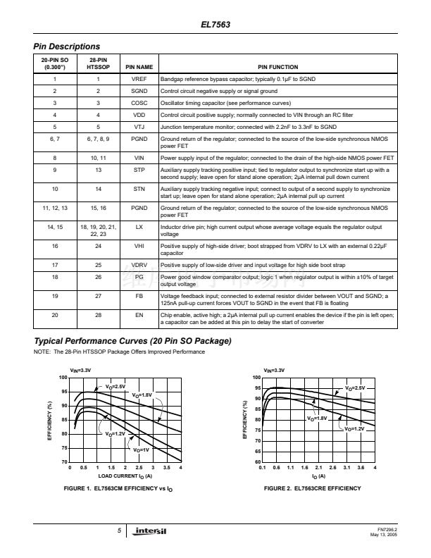 5
5
 6
6
 7
7
 8
8
 9
9
 10
10
 11
11
 12
12
 13
13
 14
14
 15
15
 16
16
