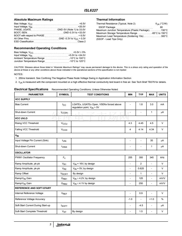
ISL6227
Functional Pin Description
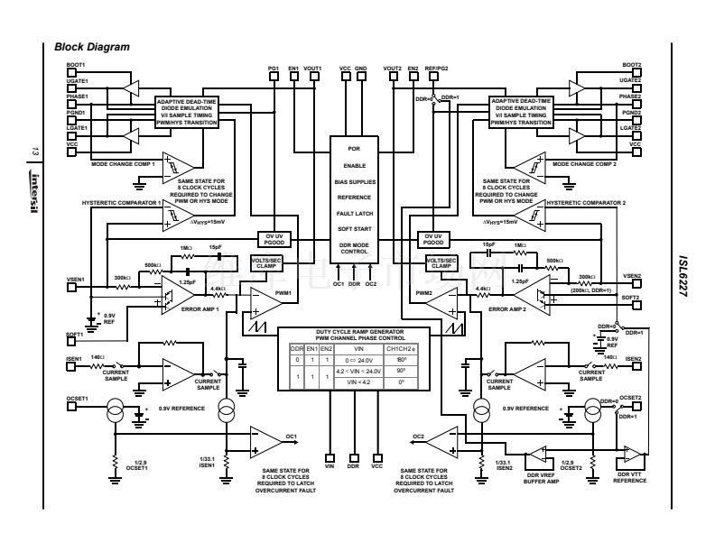
GND (Pin 1)
Signal ground for the IC.
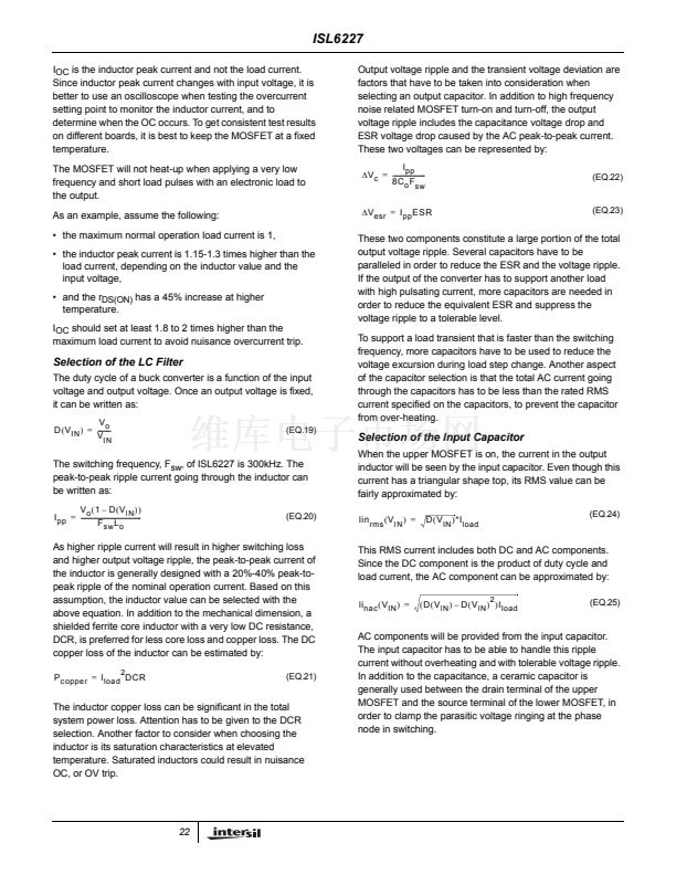
OCSET1 (Pin 11)
This pin is a buffered 0.9V internal reference voltage. A
resistor from this pin to ground sets the overcurrent
threshold for the first controller.
LGATE1, LGATE2 (Pin 2, 27)
These are the outputs of the lower MOSFET drivers.
SOFT1, SOFT2 (Pin 12, 17)
These pins provide soft-start function for their respective
controllers. When the chip is enabled, the regulated 4.5碌A
pull-up current source charges the capacitor connected from
the pin to ground. The output voltage of the converter follows
the ramping voltage on the SOFT pin in the soft-start
process with the SOFT pin voltage as reference. When the
SOFT pin voltage is higher than 0.9V, the error amplifier will
use the internal 0.9V reference to regulate output voltage.
In the event of undervoltage and overcurrent shutdown, the
soft-start pin is pulled down though a 2K resistor to ground to
discharge the soft-start capacitor.
PGND1, PGND2 (Pin 3, 26)
These pins provide the return connection for lower gate
drivers, and are connected to sources of the lower
MOSFETs of their respective converters.
PHASE1, PHASE2 (Pin 4, 25)
The PHASE1 and PHASE2 points are the junction points of
the upper MOSFET sources, output filter inductors, and
lower MOSFET drains. Connect these pins to the respective
converter鈥檚 upper MOSFET source.
UGATE1, UGATE2 (Pin 5, 24)
These pins provide the gate drive for the upper MOSFETs.
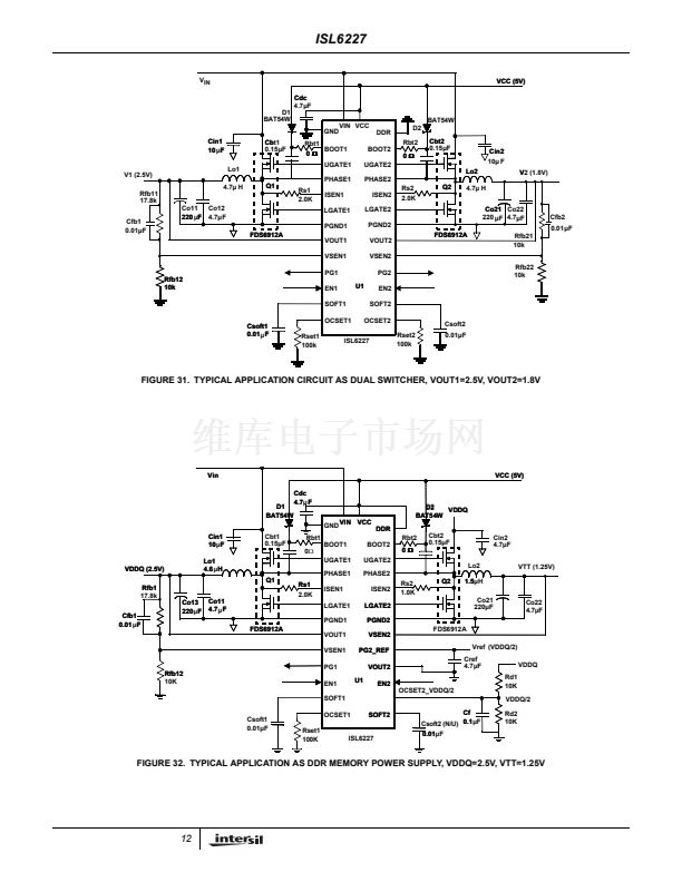
DDR (Pin 13)
When the DDR pin is low, the chip can be used as a dual
switcher controller. The output voltage of the two channels
can be programmed independently by VSENx pin resistor
dividers. The PWM signals of channel 1 and channel 2 will
be synchronized 180 degrees out-of-phase. When the DDR
pin is high, the chip transforms into a complete DDR memory
solution. The OCSET2 pin becomes an input through a
resistor divider tracking to VDDQ/2. The PG2/REF pin
becomes the output of the VDDQ/2 buffered voltage. The
VDDQ/2 voltage is also used as the reference to the error
amplifier by the second channel. The channel phase-shift
synchronization is determined by the VIN pin when DDR=1
as described in VIN (Pin 14) below.
BOOT1, BOOT2 (Pin 6, 23)
These pins power the upper MOSFET drivers of the PWM
converter. Connect this pin to the junction of the bootstrap
capacitor with the cathode of the bootstrap diode. The anode
of the bootstrap diode is connected to the VCC voltage.
ISEN1, ISEN2 (Pin 7, 22)
These pins are used to monitor the voltage drop across the
lower MOSFET for current feedback and Overcurrent
protection. For precise current detection these inputs can be
connected to the optional current sense resistors placed in
series with the source of the lower MOSFETs.
EN1, EN2 (Pin 8, 21)
These pins enable operation of the respective converter
when high. When both pins are low, the chip is disabled and
only low leakage current is taken from VCC and VIN. EN1
and EN2 can be used independently to enable either
channel 1 or channel 2.
VIN (Pin 14)
This pin has multiple functions. When connected to battery
voltage, it provides battery voltage to the oscillator as a feed-
forward for the rejection of input voltage variation. The ramp
of the PWM comparator is proportional to the voltage on this
pin (see Table 1 and Table 2 for details). While the DDR pin
is high in the DDR application, and when the VIN pin voltage
is greater than 4.2 volt when connecting to a battery, it
commands 90掳 out-of-phase channel synchronization, with
the second channel lagging the first channel, to reduce inter-
channel interference. When the pin voltage is less than 4.2V,
this pin commands in-phase channel synchronization.
VOUT1, VOUT2 (Pin 9, 20)
These pins, when connected to the converter鈥檚 respective
outputs, set the converter operating in a mixed hysteretic
mode or PWM mode, depending on the load conditions. It
also provides the voltage to the chip to clamp the PWM error
amplifier in hysteretic mode to achieve smooth HYS/PWM
transition. When connected to ground, these pins command
forced continuous conduction mode (PWM) at all load levels.
PG1 (Pin 15)
PGOOD1 is an open drain output used to indicate the status
of the output voltage. This pin is pulled low when the first
channel output is out of -11% -- +15% of the set value.
VSEN1, VSEN2 (Pin 10, 19)
These pins are connected to the resistive dividers that set
the desired output voltage. The PGOOD, UVP, and OVP
circuits use this signal to report output voltage status.
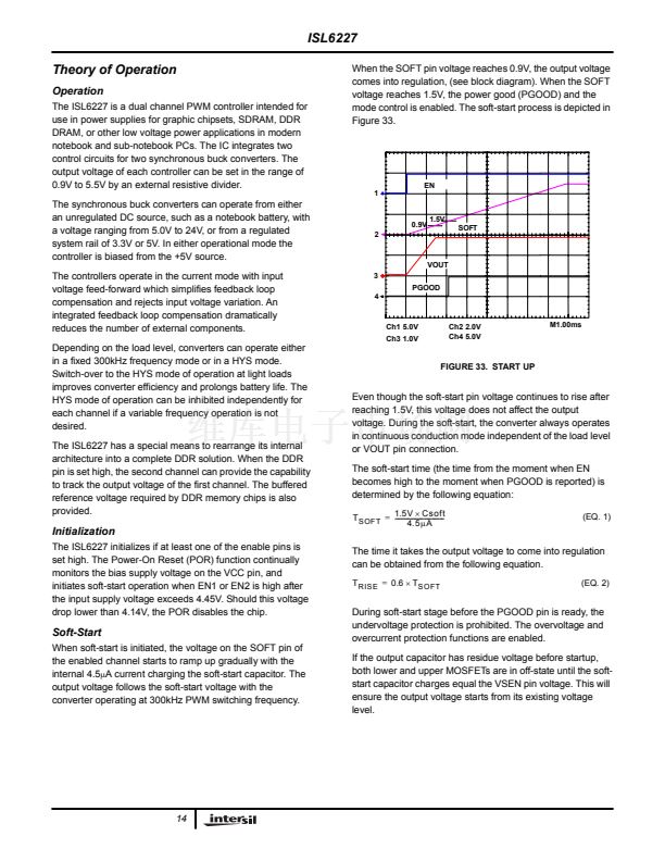
10


 1
1
 2
2
 3
3
 4
4
 5
5
 6
6
 7
7
 8
8
 9
9
 10
10
 11
11
 12
12
 13
13
 14
14
 15
15
 16
16
 17
17
 18
18
 19
19
 20
20
 21
21
 22
22
 23
23
 24
24
 25
25
 26
26
