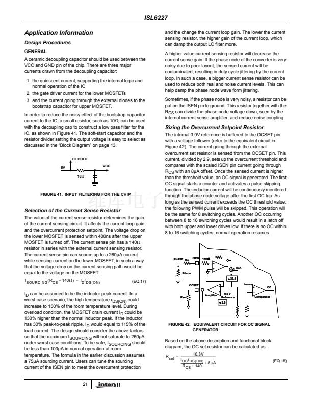
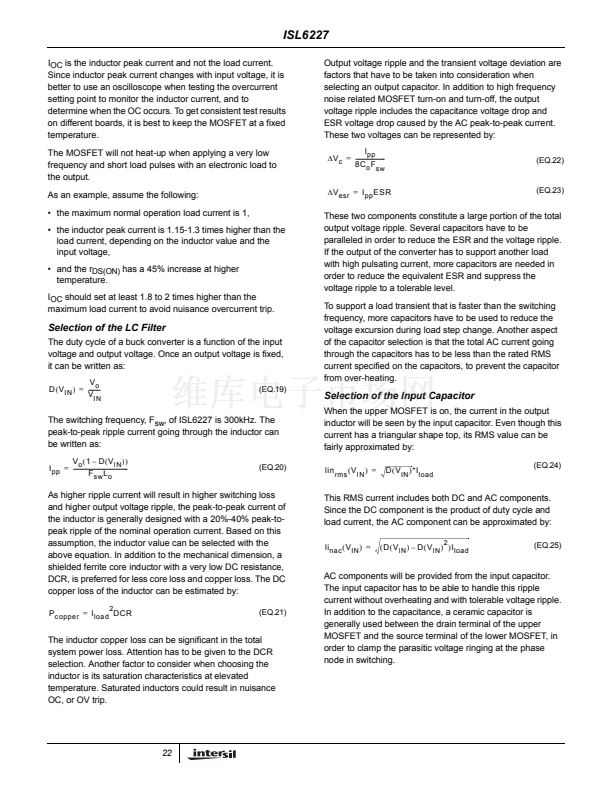
ISL6227
Tuning the Turn-on of Upper MOSFET
The turn-on speed of the upper MOSFET can be adjusted by
the resistor connecting the boot cap to the BOOT pin of the
chip. This resistor can confine the voltage ringing on the boot
capacitor from coupling to the boot pin. This resistor slows
down only the turn-on of the upper MOSFET.
If the upper MOSFET is turned on very fast, it could result in
a very high dv/dt on the phase node, which could couple into
the lower MOSFET gate through the miller capacitor,
causing momentous shoot-through. This phenomenon,
together with the reverse recovery of the body diode of the
lower MOSFET, can over-shoot the phase node voltage to
beyond the voltage rating of the MOSFET. However, a bigger
resistor will slow the turn-on of the MOSFET too much and
lower the efficiency. Trade-offs need to be made in choosing
a suitable resistor value.
the opposite side of the board. For example, prospective
layer arrangement on a 4 layer board is shown below:
1. Top Layer: ISL6227 signal lines
2. Signal Ground
3. Power Layers: Power Ground
4. Bottom Layer: Power MOSFET, Inductors and other
Power traces
It is a good engineering practice to separate the power
voltage and current flowing path from the control and logic
level signal path. The controller IC will stay on the signal
layer, which is isolated by the signal ground to the power
signal traces.
Component Placement
The control pins of the two-channel ISL6227 are located
symmetrically on two sides of the IC; it is desirable to
arrange the two channels symmetrically around the IC.
The power MOSFET should be close to the IC so that the
gate drive signal, the LGATEx, UGATEx, PHASEx, BOOTx,
and ISENx traces can be short.
Place the components in such a way that the area under the
ISL6227 has fewer noise traces with high dv/dt and di/dt,
such as gate signals and phase node signals.
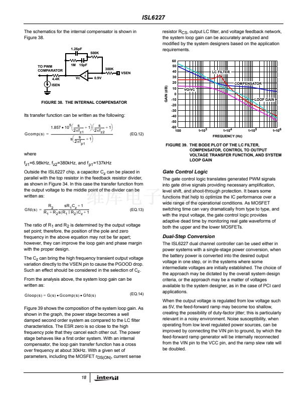
System Loop Gain and Stability
The system loop gain is a product of three transfer functions:
1. the transfer function from the output voltage to the
feedback point,
2. the transfer function of the internal compensation circuit
from the feedback point to the error amplifier output voltage,
3. and the transfer function from the error amplifier output to
the converter output voltage.
These transfer functions are written in a closed form in the
Theory of Operation section on page 18. The external
capacitor, in parallel with the upper resistor of the resistor
divider, C
z
, can be used to tune the loop gain and phase
margin. Other component parameters, such as the inductor
value, can be changed for a wider cross-over frequency of the
system loop gain. A body plot of the loop gain transfer function
with a 45 degree phase margin (a 60 degree phase margin is
better) is desirable to cover component parameter variations.
Signal Ground and Power Ground Connection
At minimum, a reasonably large area of copper, which will
shield other noise couplings through the IC, could be used
as signal ground beneath the ISL6227. The best tie-point
between the signal ground and the power ground is at the
negative side of the output capacitor on each channel, where
there is less noise. Noisy traces beneath the ISL6227 are
not recommended.
Pin 1 and Pin 28, the GND and VCC
At least one high quality ceramic decoupling cap should be
used across these two pins. A via can tie Pin 1 to signal
ground. Since Pin1 and Pin 28 are close together, the
decoupling cap can be put close to the IC.
Testing the Overvoltage on Buck Converters
For synchronous buck converters, if an active source is used
to raise the output voltage for the overvoltage protection test,
the buck converter will behave like a boost converter and
dump energy from the external source to the input. The
overvoltage test can be done on ISL6227 by connecting the
VSEN pin to an external voltage source or signal generator
through a diode. When the external voltage, or signal
generator voltage, is tuned to a higher level than the
overvoltage threshold (the lower MOSFET will be on), it
indicates the overvoltage protection works. This kind of
overvoltage protection does not require an external schottky
in parallel with the output capacitor.
Pin 2 and Pin 27, the LGATE1 and LGATE2
These are the gate drive signals for the bottom MOSFETs of
the buck converter. The signal going through these traces
have both high dv/dt and high di/dt, with high peak charging
and discharging current. These two traces should be short,
wide, and away from other traces. There should be no other
weak signal traces in parallel with these traces on any layer.
Pin 3 and Pin 26, the PGND1 and PGND2
Each pin should be laid out to the negative side of the
relevant output cap with separate traces.The negative side
of the output capacitor must be close to the source node of
the bottom MOSFET. These traces are the return path of
LGATE1 and LGATE2.
Layout Considerations
Power and Signal Layer Placement on the PCB
As a general rule, power layers should be close together,
either on the top or bottom of the board, with signal layers on
24


 1
1
 2
2
 3
3
 4
4
 5
5
 6
6
 7
7
 8
8
 9
9
 10
10
 11
11
 12
12
 13
13
 14
14
 15
15
 16
16
 17
17
 18
18
 19
19
 20
20
 21
21
 22
22
 23
23
 24
24
 25
25
 26
26
