鈥?/div>
V
IN
(EQ.16)
As seen from the equation above, the inductor peak current
changes with the input voltage and the inductor value once
an output voltage is selected.
After overcurrent protection is activated, there are two ways
to bring the offending channel back: (1) Both EN1 and EN2
have to be held low to clear the latch, (2) To recycle the Vcc
of the chip, the POR will clear the latch.
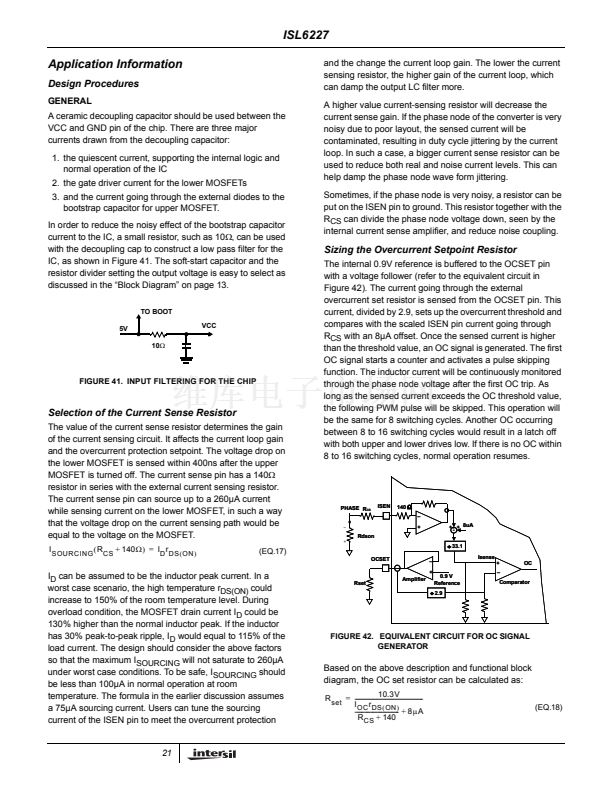
where, I
OC
is a desired overcurrent protection threshold and
R
CS
is the value of the current sense resistor connected to
the ISEN pin. The 8碌A is the offset current added on top of
the sensed current from the ISEN pin for internal circuit
biasing.
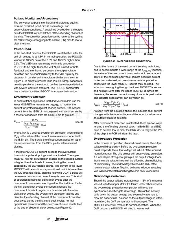
If the lower MOSFET current exceeds the overcurrent
threshold, a pulse skipping circuit is activated. The upper
MOSFET will not be turned on as long as the sensed current
is higher than the threshold value, limiting the current
supplied by the DC voltage source. The current in the lower
MOSFET will be continuously monitored until it is lower than
the OC threshold value, then the following UGATE pulse will
be released and normal current sample resumes. This kind
of operation remains for eight clock cycles after the
overcurrent comparator was tripped for the first time. If after
the first eight clock cycles the current exceeds the
overcurrent threshold again, in a time interval of another
eight clock cycles, the overcurrent protection latches and
disables the offending channel. If the overcurrent condition
goes away during the first eight clock cycles, normal
operation is restored and the overcurrent circuit resets itself
at the end of sixteenth clock cycles; see Figure 40.
Undervoltage Protection
In the process of operation, if a short circuit occurs, the output
voltage will drop quickly. Before the overcurrent protection
circuit responds, the output voltage will fall out of the required
regulation range. The chip comes with undervoltage protection.
If a load step is strong enough to pull the output voltage lower
than the undervoltage threshold, the offending channel latches
off immediately. The undervoltage threshold is 75% of the
nominal output voltage. Toggling both pins to low, or recycling
Vcc, will clear the latch and bring the chip back to operation.
Overvoltage Protection
Should the output voltage increase over 115% of the normal
value due to the upper MOSFET failure, or for other reasons,
the overvoltage protection comparator will force the
synchronous rectifier gate driver high. This action actively
pulls down the output voltage and eventually attempts to
blow the battery fuse. As soon as the output voltage is within
regulation, the OVP comparator is disengaged. The
MOSFET driver will restore its normal operation. When the
OVP occurs, the PGOOD will drop to low as well.
19


 1
1
 2
2
 3
3
 4
4
 5
5
 6
6
 7
7
 8
8
 9
9
 10
10
 11
11
 12
12
 13
13
 14
14
 15
15
 16
16
 17
17
 18
18
 19
19
 20
20
 21
21
 22
22
 23
23
 24
24
 25
25
 26
26
