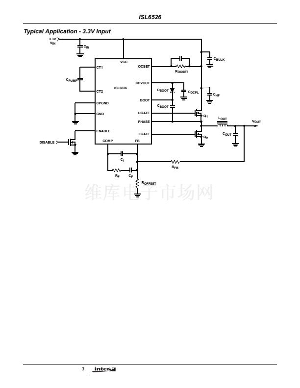
铮?/div>
1
-
F
P2
= -----------------------------------
2蟺 x R
3
x C
3
1
F
Z2
= ------------------------------------------------------
-
2蟺 x
(
R
1
+
R
3
)
x C
3
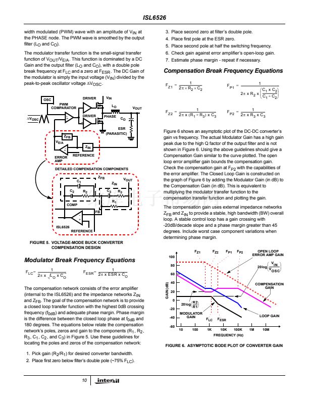
Z
FB
V
E/A
-
+
ERROR
AMP
Z
IN
REFERENCE
ESR
(PARASITIC)
DETAILED COMPENSATION COMPONENTS
C
1
C
2
R
2
Z
FB
Z
IN
C
3
R
1
FB
R
3
V
OUT
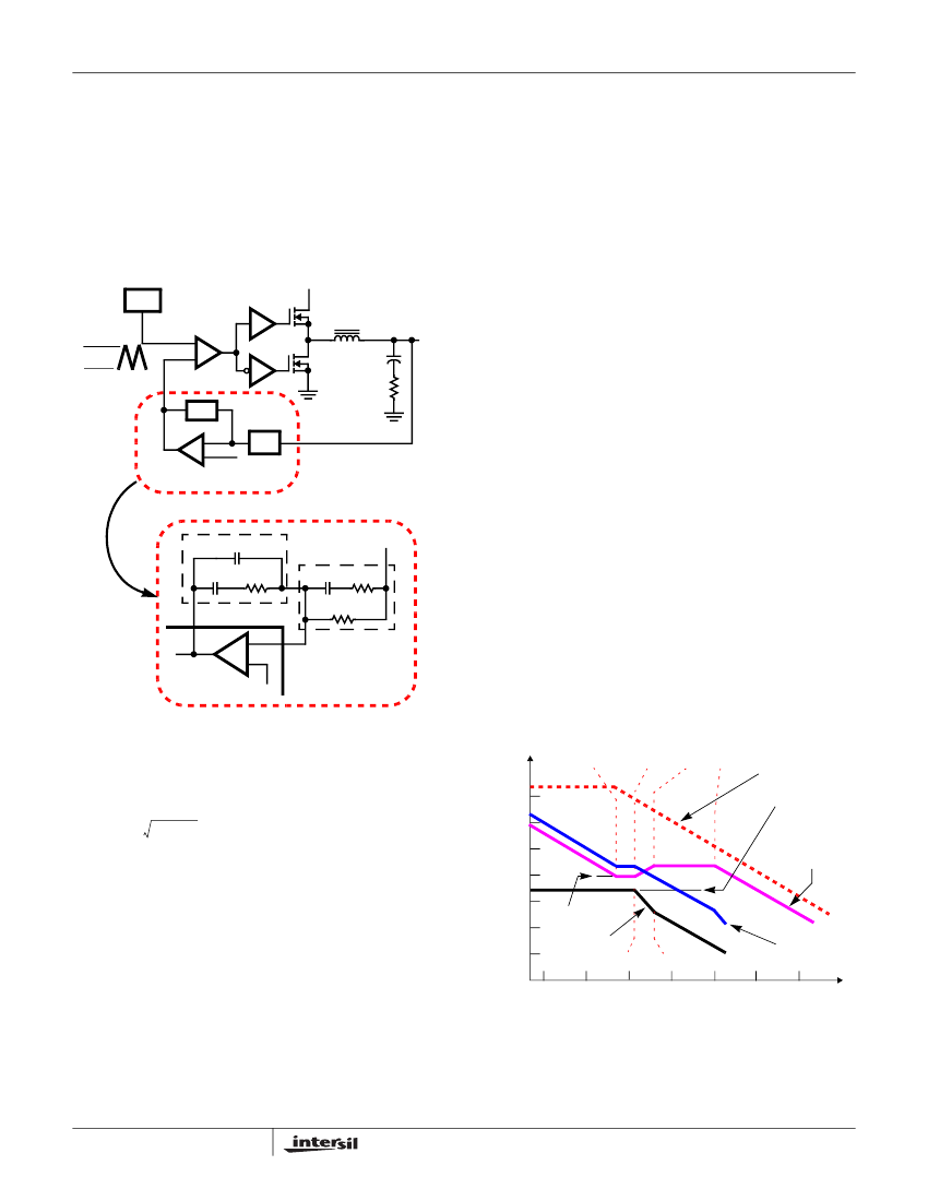
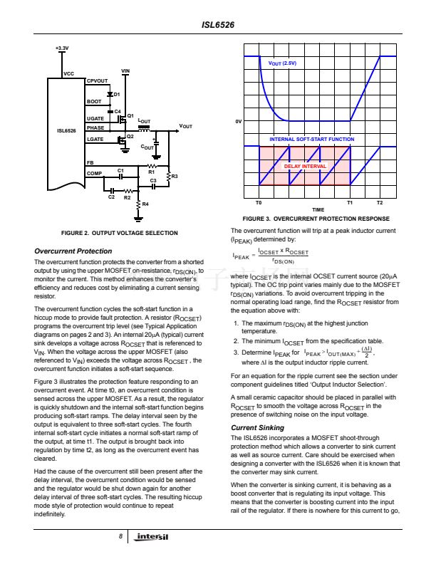
Figure 6 shows an asymptotic plot of the DC-DC converter鈥檚
gain vs frequency. The actual Modulator Gain has a high gain
peak due to the high Q factor of the output filter and is not
shown in Figure 6. Using the above guidelines should give a
Compensation Gain similar to the curve plotted. The open
loop error amplifier gain bounds the compensation gain.
Check the compensation gain at F
P2
with the capabilities of
the error amplifier. The Closed Loop Gain is constructed on
the graph of Figure 6 by adding the Modulator Gain (in dB) to
the Compensation Gain (in dB). This is equivalent to
multiplying the modulator transfer function to the
compensation transfer function and plotting the gain.
The compensation gain uses external impedance networks
Z
FB
and Z
IN
to provide a stable, high bandwidth (BW) overall
loop. A stable control loop has a gain crossing with
-20dB/decade slope and a phase margin greater than 45
degrees. Include worst case component variations when
determining phase margin.
F
Z1
100
80
F
Z2
F
P1
F
P2
OPEN LOOP
ERROR AMP GAIN
铮?/div>
V IN
铮?/div>
-
20 log
铮?/div>
-----------------
铮?/div>
铮?/div>
V OSC
铮?/div>
COMP
-
+
ISL6526
REFERENCE
FIGURE 5. VOLTAGE-MODE BUCK CONVERTER
COMPENSATION DESIGN
Modulator Break Frequency Equations
1
F
LC
= -----------------------------------------
-
2蟺 x L
O
x C
O
1
F
ESR
= ------------------------------------------
-
2蟺 x ESR x C
O
60
GAIN (dB)
40
20
0
-20
-40
-60
R2
-
20 log
铮?/div>
-------
铮?/div>
铮?/div>
R1
铮?/div>
MODULATOR
GAIN
10
100
F
LC
1K
F
ESR
10K
100K
1M
The compensation network consists of the error amplifier
(internal to the ISL6526) and the impedance networks Z
IN
and Z
FB
. The goal of the compensation network is to provide
a closed loop transfer function with the highest 0dB crossing
frequency (f
0dB
) and adequate phase margin. Phase margin
is the difference between the closed loop phase at f
0dB
and
180 degrees. The equations below relate the compensation
network鈥檚 poles, zeros and gain to the components (R
1
, R
2
,
R
3
, C
1
, C
2
, and C
3
) in Figure 5. Use these guidelines for
locating the poles and zeros of the compensation network:
1. Pick gain (R
2
/R
1
) for desired converter bandwidth.
2. Place first zero below filter鈥檚 double pole (~75% F
LC
).
COMPENSATION
GAIN
LOOP GAIN
10M
FREQUENCY (Hz)
FIGURE 6. ASYMPTOTIC BODE PLOT OF CONVERTER GAIN
10
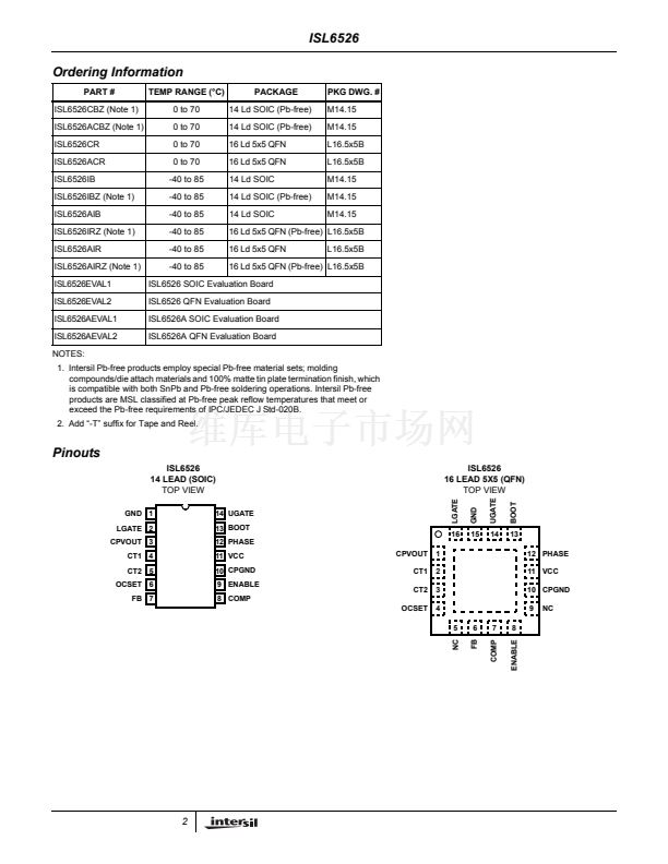
ISL6526CB 产品属性
500
集成电路 (IC)
PMIC - 稳压器 - DC DC 切换控制器
-
电压模式
1
325kHz
100%
2.97 V ~ 3.63 V
是
无
无
无
无
无
无
无
0°C ~ 70°C
14-SOIC(0.154",3.90mm 宽)
管件
ISL6526CB相关型号PDF文件下载
-
型号
版本
描述
厂商
下载
-
英文版
Current Regulated PCI Hot Plug Power Switch Controller
-
英文版
Dual Slot PCI-Express Power Controller
-
英文版
Dual Slot PCI-E Hot Plug Controllers
-
英文版
Power Distribution Controllers
-
英文版
Power Distribution Controllers
-
英文版
Power Distribution Controllers
-
英文版
Dual Power Supply Controller
-
英文版
USB Dual Port Power Supply Controller
-
英文版
Power Distribution Controllers
-
英文版
Single Supply Integrated Current Limiting Controller
-
英文版
Power Sequencing Controllers
-
英文版
Power Sequencing Controllers
-
英文版
Power Sequencing Controllers
-
英文版
Power Sequencing Controllers
-
英文版
Power Sequencing Controllers
-
英文版
Power Sequencing Controllers
-
英文版
Power Sequencing Controllers
-
英文版
Power Sequencing Controllers
INTERSIL [Inter...
-
英文版
Multiple Voltage Supervisory ICs
-
英文版
Multiple Voltage Supervisory ICs
INTERSIL [...


 1
1
 2
2
 3
3
 4
4
 5
5
 6
6
 7
7
 8
8
 9
9
 10
10
 11
11
 12
12
 13
13
 14
14
 15
15
