ISL6526
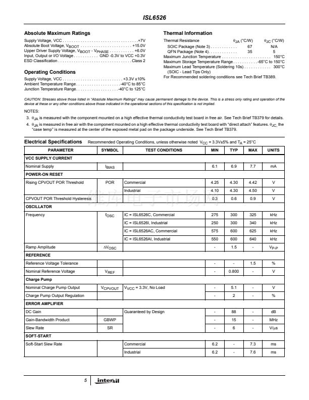
Electrical Specifications
PARAMETER
GATE DRIVERS
Upper Gate Source Current
Upper Gate Sink Current
Lower Gate Source Current
Lower Gate Sink Current
PROTECTION/DISABLE
OCSET Current Source
I
OCSET
Commercial
Industrial
Disable Threshold
V
DISABLE
18
16
-
20
20
-
22
22
0.8
碌A
碌A
V
I
UGATE-SRC
V
BOOT
- V
PHASE
= 5V, V
UGATE
= 4V
I
UGATE-SNK
I
LGATE-SRC
V
VCC
= 3.3V, V
LGATE
= 4V
I
LGATE-SNK
-
-
-
-
-1
1
-1
2
-
-
-
-
A
A
A
A
Recommended Operating Conditions, unless otherwise noted V
CC
= 3.3V卤5% and T
A
= 25掳C
(Continued)
SYMBOL
TEST CONDITIONS
MIN
TYP
MAX
UNITS
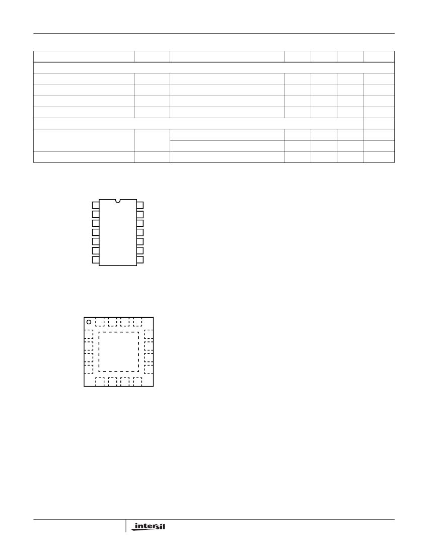
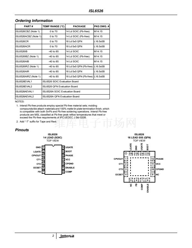
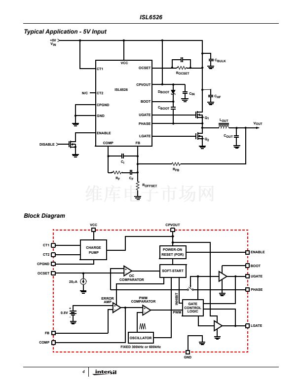
Functional Pin Description
14 LEAD (SOIC)
TOP VIEW
GND 1
LGATE 2
CPVOUT 3
CT1 4
CT2 5
OCSET 6
FB 7
14 UGATE
13 BOOT
12 PHASE
11 VCC
10 CPGND
9 ENABLE
8 COMP
GND
This pin represents the signal and power ground for the IC.
Tie this pin to the ground island/plane through the lowest
impedance connection available.
PHASE
Connect this pin to the upper MOSFET鈥檚 source. This pin is
used to monitor the voltage drop across the upper MOSFET
for overcurrent protection.
UGATE
Connect this pin to the upper MOSFET鈥檚 gate. This pin
provides the PWM-controlled gate drive for the upper
MOSFET. This pin is also monitored by the adaptive shoot-
through protection circuitry to determine when the upper
MOSFET has turned off.
16 LEAD 5X5 (QFN)
TOP VIEW
UGATE
LGATE
BOOT
GND
BOOT
This pin provides ground referenced bias voltage to the
upper MOSFET driver. A bootstrap circuit is used to create a
voltage suitable to drive a logic-level N-Channel MOSFET.
16
CPVOUT
CT1
CT2
OCSET
1
2
3
4
5
NC
15
14
13
12 PHASE
11 VCC
10 CPGND
9
NC
LGATE
Connect this pin to the lower MOSFET鈥檚 gate. This pin
provides the PWM-controlled gate drive for the lower
MOSFET. This pin is also monitored by the adaptive shoot-
through protection circuitry to determine when the lower
MOSFET has turned off.
6
FB
7
COMP
8
ENABLE
OCSET
Connect a resistor (R
OCSET
) from this pin to the drain of the
upper MOSFET (V
IN
). R
OCSET
, an internal 20碌A current
source (I
OCSET
), and the upper MOSFET on-resistance
(r
DS(ON)
) set the converter overcurrent (OC) trip point
according to the following equation:
I
OCSET
xR
OCSET
I
PEAK
= -------------------------------------------------
r
DS
(
ON
)
VCC
This pin provides the bias supply for the ISL6526. Connect a
well-decoupled 3.3V supply to this pin.
COMP and FB
COMP and FB are the available external pins of the error
amplifier. The FB pin is the inverting input of the internal
error amplifier and the COMP pin is the error amplifier
output. These pins are used to compensate the voltage-
control feedback loop of the converter.
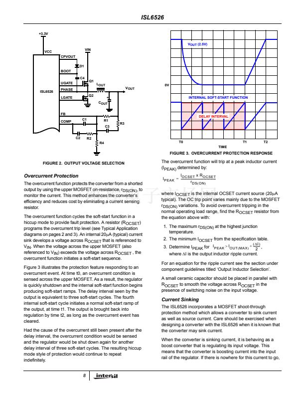
An overcurrent trip cycles the soft-start function.
6


 1
1
 2
2
 3
3
 4
4
 5
5
 6
6
 7
7
 8
8
 9
9
 10
10
 11
11
 12
12
 13
13
 14
14
 15
15
