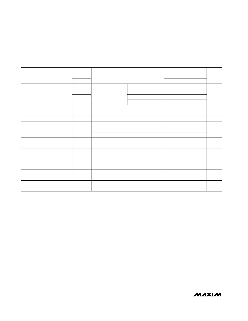
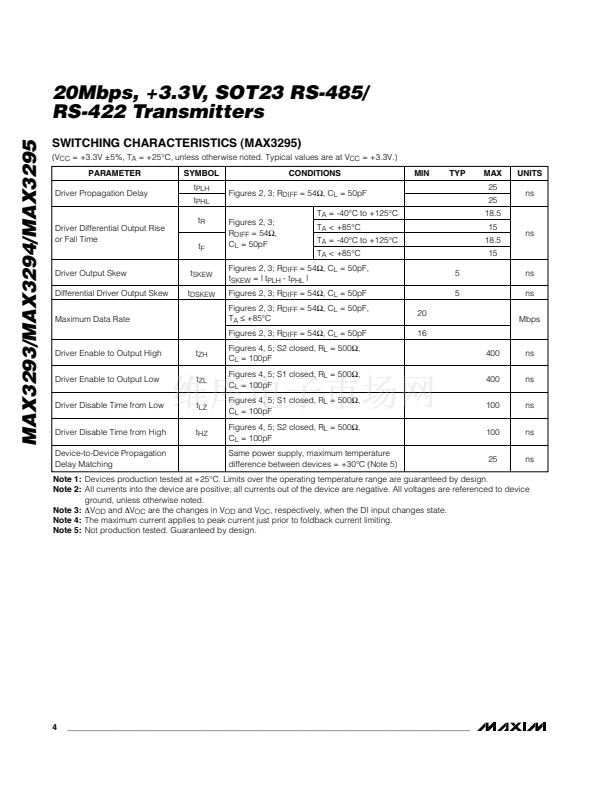
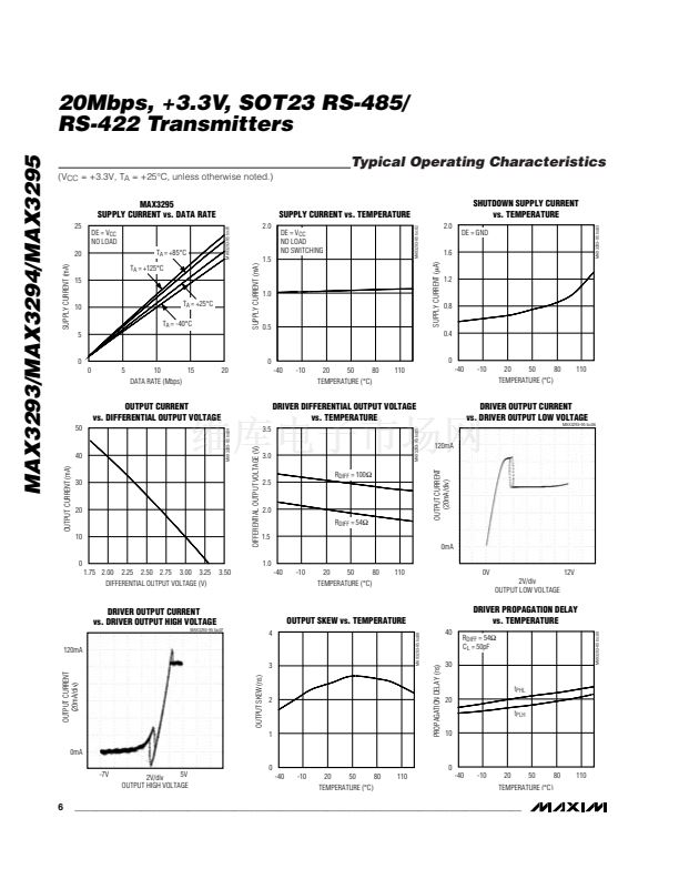
= +25掳C, unless otherwise noted. Typical values are at V
鈮?/div>
+85掳C
Figures 2, 3; R
DIFF
= 54鈩? C
L
= 50pF
Driver Enable to Output High
Driver Enable to Output Low
Driver Disable Time from Low
Driver Disable Time from High
Device-to-Device Propagation
Delay Matching
t
ZH
t
ZL
t
LZ
t
HZ
Figures 4, 5; S2 closed, R
L
= 500鈩?
C
L
= 100pF
Figures 4, 5; S1 closed, R
L
= 500鈩?
C
L
= 100pF
Figures 4, 5; S1 closed, R
L
= 500鈩?
C
L
= 100pF
Figures 4, 5; S2 closed, R
L
= 500鈩?
C
L
= 100pF
Same power supply, maximum temperature
difference between devices = +30掳C (Note 5)
20
16
400
400
100
100
25
ns
ns
ns
ns
ns
5
5
MIN
TYP
MAX
25
25
18.5
15
18.5
15
ns
ns
Mbps
ns
UNITS
ns
Driver Differential Output Rise
or Fall Time
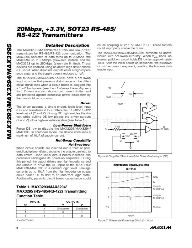
Note 1:
Devices production tested at +25掳C. Limits over the operating temperature range are guaranteed by design.
Note 2:
All currents into the device are positive; all currents out of the device are negative. All voltages are referenced to device
ground, unless otherwise noted.
Note 3:
鈭哣
OD
and
鈭哣
OC
are the changes in V
OD
and V
OC
, respectively, when the DI input changes state.
Note 4:
The maximum current applies to peak current just prior to foldback current limiting.
Note 5:
Not production tested. Guaranteed by design.
4
_______________________________________________________________________________________


 1
1
 2
2
 3
3
 4
4
 5
5
 6
6
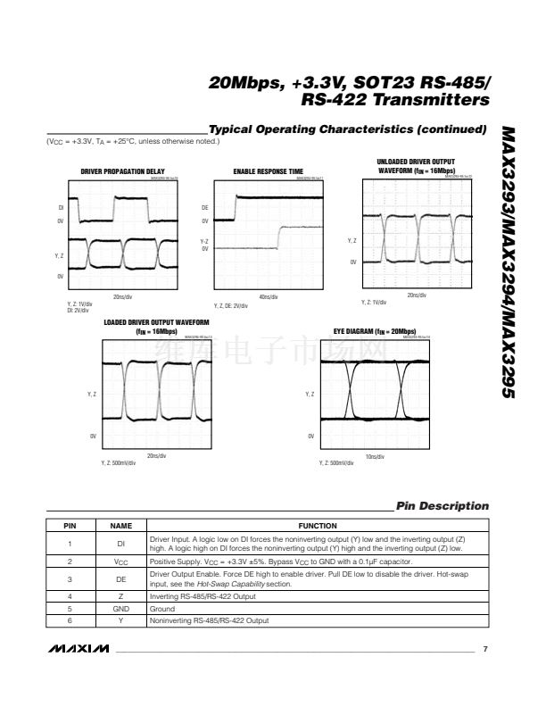 7
7
 8
8
 9
9
 10
10
 11
11
