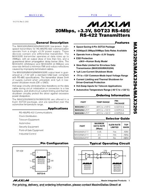
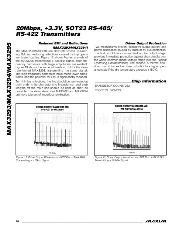
20Mbps, +3.3V, SOT23 RS-485/
RS-422 Transmitters
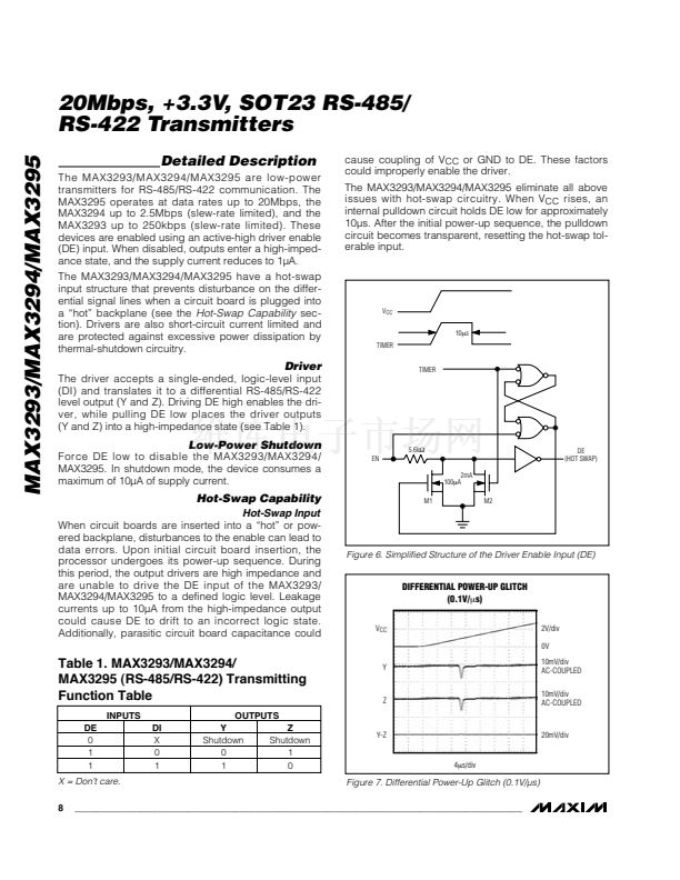
Hot-Swap Input Circuitry
The MAX3293/MAX3294/MAX3295 enable input fea-
tures hot-swap capability. At the input, there are two
NMOS devices, M1 and M2 (Figure 6). When V
CC
ramps from zero, an internal 10碌s timer turns on M2
and sets the SR latch, which also turns on M1.
Transistors M2, a 2mA current sink, and M1, a 100碌A
current sink, pull DE to GND through a 5.6k鈩?resistor.
M2 is designed to pull DE to the disabled state against
an external parasitic capacitance up to 100pF that may
drive DE high. After 10碌s, the timer deactivates M2
while M1 remains on, holding DE low against three-
state leakages that can drive DE high. M1 remains on
until an external source overcomes the required input
current. At this time, the SR latch resets and M1 turns
DIFFERENTIAL POWER-UP GLITCH
(1V/碌s)
V
CC
2V/div
0V
100mV/div
AC-COUPLED
100mV/div
AC-COUPLED
off. When M1 turns off, DE reverts to a standard, high-
impedance CMOS input. Whenever V
CC
drops below
1V, the hot-swap input is reset.
MAX3293/MAX3294/MAX3295
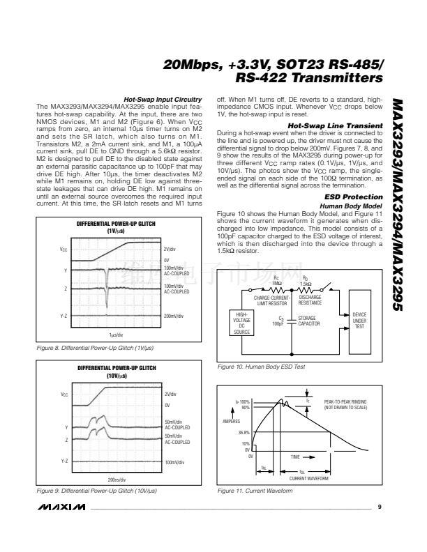
Hot-Swap Line Transient
During a hot-swap event when the driver is connected to
the line and is powered up, the driver must not cause the
differential signal to drop below 200mV. Figures 7, 8, and
9 show the results of the MAX3295 during power-up for
three different V
CC
ramp rates (0.1V/碌s, 1V/碌s, and
10V/碌s). The photos show the V
CC
ramp, the single-
ended signal on each side of the 100鈩?termination, as
well as the differential signal across the termination.
ESD Protection
Human Body Model
Figure 10 shows the Human Body Model, and Figure 11
shows the current waveform it generates when dis-
charged into low impedance. This model consists of a
100pF capacitor charged to the ESD voltage of interest,
which is then discharged into the device through a
1.5k鈩?resistor.
Y
R
C
1M鈩?/div>
CHARGE-CURRENT-
LIMIT RESISTOR
R
D
1.5k鈩?/div>
DISCHARGE
RESISTANCE
STORAGE
CAPACITOR
DEVICE
UNDER
TEST
Z
Y-Z
200mV/div
1碌s/div
HIGH-
VOLTAGE
DC
SOURCE
Cs
100pF
Figure 8. Differential Power-Up Glitch (1V/碌s)
Figure 10. Human Body ESD Test
DIFFERENTIAL POWER-UP GLITCH
(10V/碌s)
V
CC
2V/div
0V
50mV/div
AC-COUPLED
50mV/div
AC-COUPLED
I
P
100%
90%
AMPERES
36.8%
10%
0V
0V
t
RL
Ir
PEAK-TO-PEAK RINGING
(NOT DRAWN TO SCALE)
Y
Z
Y-Z
TIME
t
DL
CURRENT WAVEFORM
100mV/div
200ns/div
Figure 9. Differential Power-Up Glitch (10V/碌s)
Figure 11. Current Waveform
9
_______________________________________________________________________________________


 1
1
 2
2
 3
3
 4
4
 5
5
 6
6
 7
7
 8
8
 9
9
 10
10
 11
11
