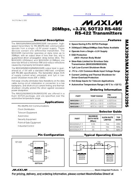
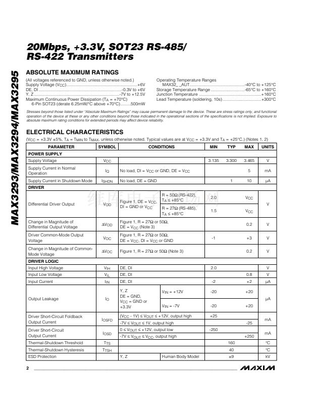
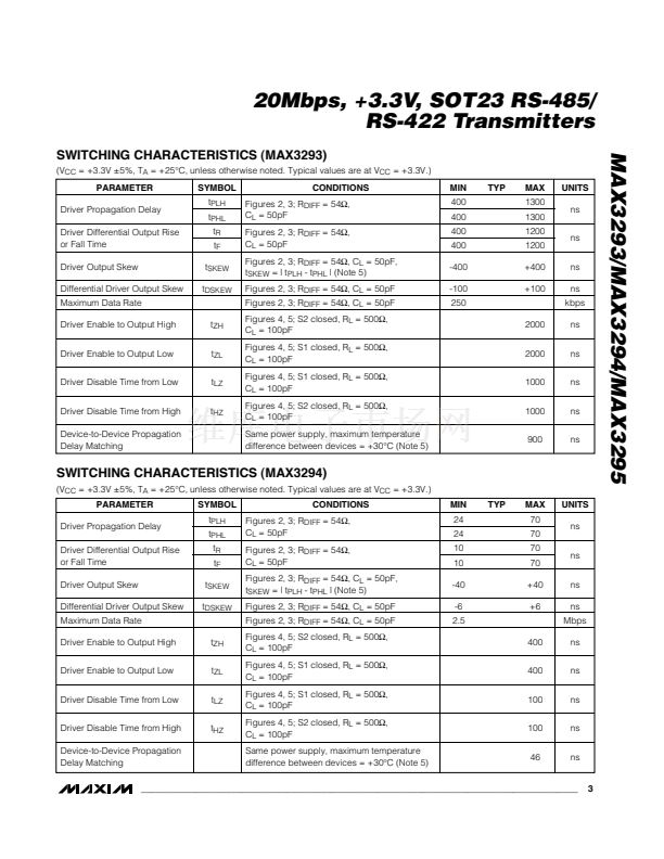
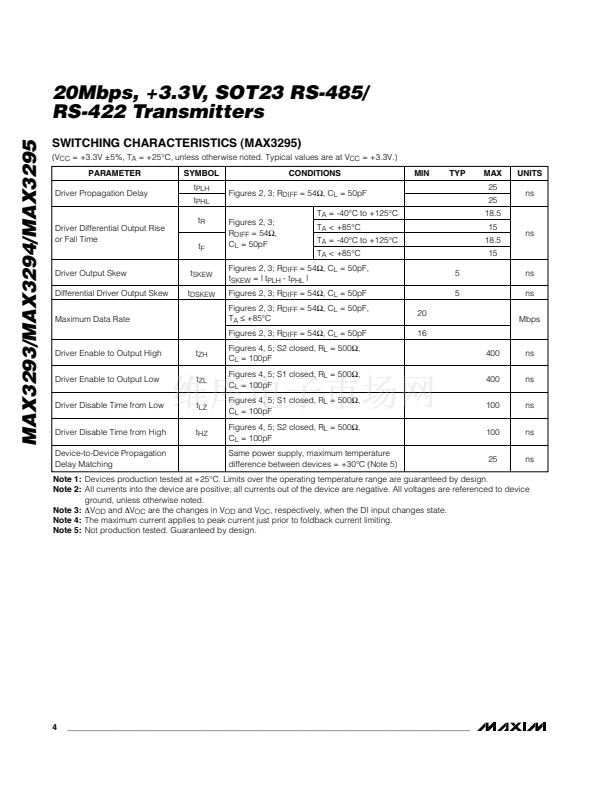
20Mbps, +3.3V, SOT23 RS-485/
RS-422 Transmitters
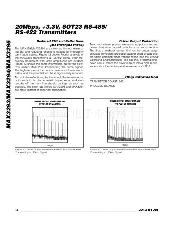
MAX3293/MAX3294/MAX3295
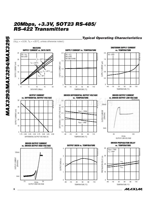
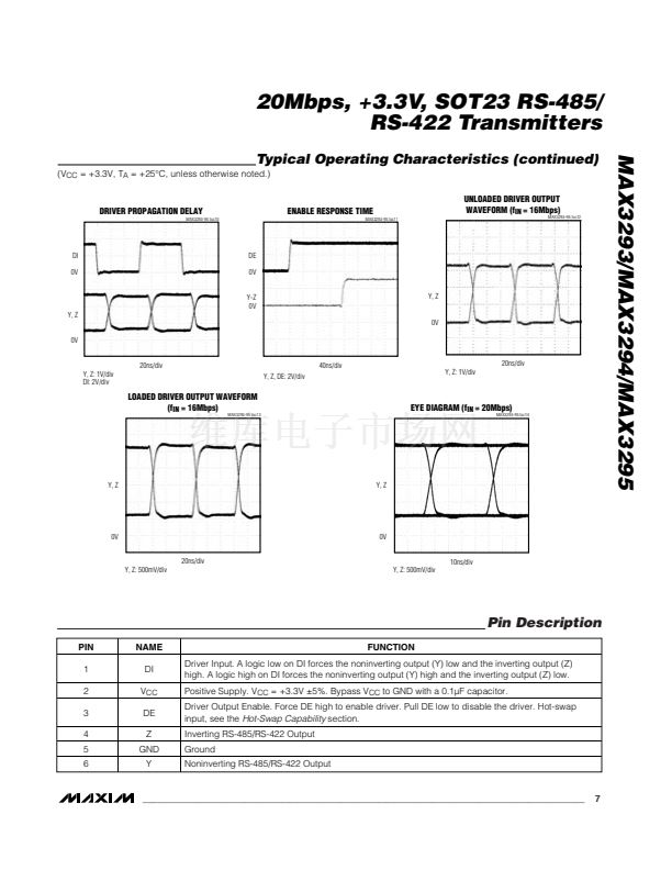
Typical Operating Characteristics (continued)
(V
CC
= +3.3V, T
A
= +25掳C, unless otherwise noted.)
UNLOADED DRIVER OUTPUT
WAVEFORM (f
IN
= 16Mbps)
MAX3293-95 toc12
DRIVER PROPAGATION DELAY
MAX3293-95 toc10
ENABLE RESPONSE TIME
MAX3293-95 toc11
DI
0V
DE
0V
Y-Z
0V
Y, Z
Y, Z
0V
0V
20ns/div
Y, Z: 1V/div
DI: 2V/div
Y, Z, DE: 2V/div
40ns/div
Y, Z: 1V/div
20ns/div
LOADED DRIVER OUTPUT WAVEFORM
(f
IN
= 16Mbps)
MAX3293-95 toc13
EYE DIAGRAM (f
IN
= 20Mbps)
MAX3293-95 toc14
Y, Z
Y, Z
0V
20ns/div
Y, Z: 500mV/div
0V
10ns/div
Y, Z: 500mV/div
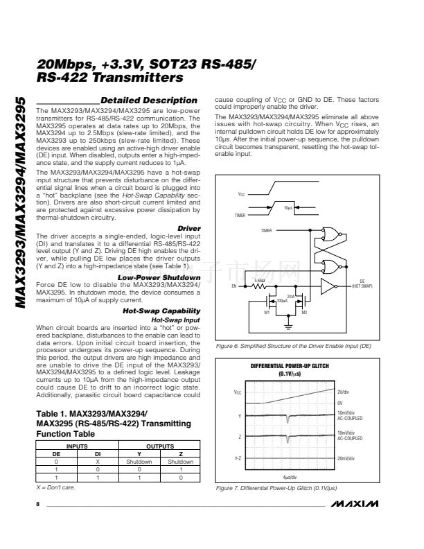
Pin Description
PIN
1
2
3
4
5
6
NAME
DI
V
CC
DE
Z
GND
Y
FUNCTION
Driver Input. A logic low on DI forces the noninverting output (Y) low and the inverting output (Z)
high. A logic high on DI forces the noninverting output (Y) high and the inverting output (Z) low.
Positive Supply. V
CC
= +3.3V 卤5%. Bypass V
CC
to GND with a 0.1碌F capacitor.
Driver Output Enable. Force DE high to enable driver. Pull DE low to disable the driver. Hot-swap
input, see the
Hot-Swap Capability
section.
Inverting RS-485/RS-422 Output
Ground
Noninverting RS-485/RS-422 Output
_______________________________________________________________________________________
7


 1
1
 2
2
 3
3
 4
4
 5
5
 6
6
 7
7
 8
8
 9
9
 10
10
 11
11
