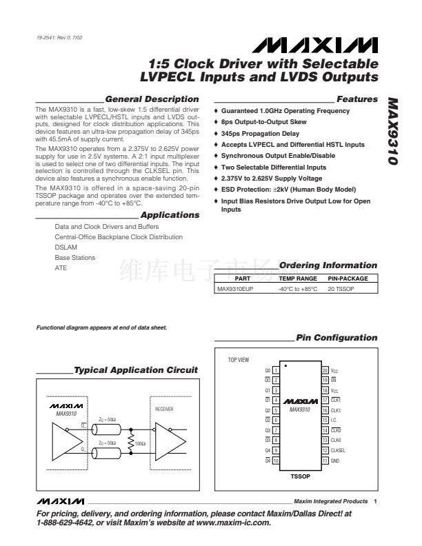
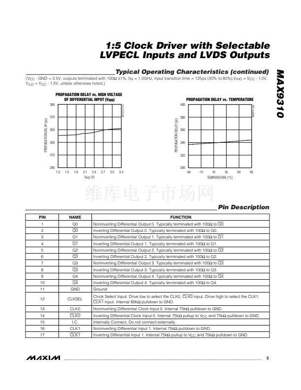
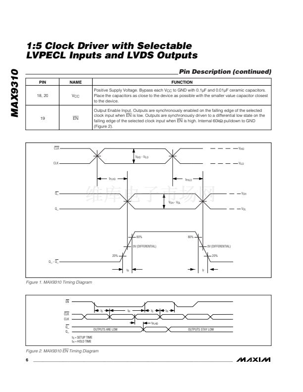
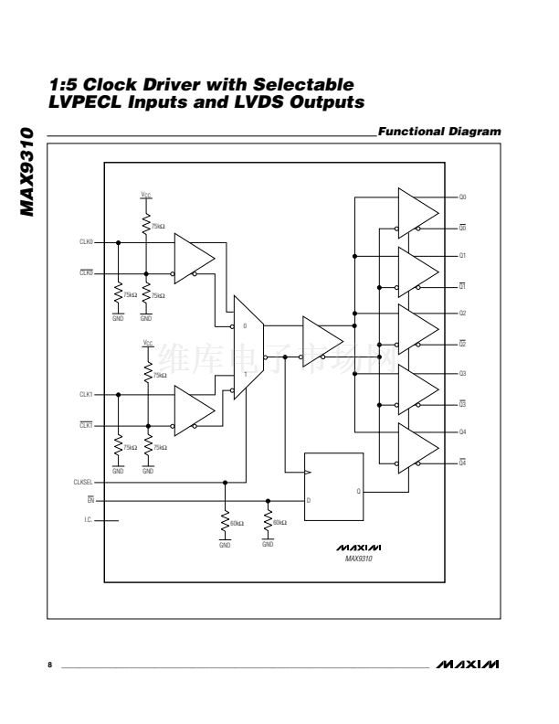
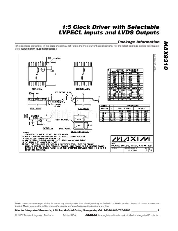
1:5 Clock Driver with Selectable
LVPECL Inputs and LVDS Outputs
MAX9310
ABSOLUTE MAXIMUM RATINGS
V
CC
to GND ...........................................................-0.3V to +4.1V
EN,
CLKSEL, CLK_,
CLK_,
to GND............-0.3V to (V
CC
+ 0.3V)
CLK_ to
CLK_
...........................................................|V
CC
- GND|
Continuous Output Current .................................................24mA
Surge Output Current..........................................................50mA
Continuous Power Dissipation (T
A
= +70掳C)
Single-Layer PC Board
20-Pin TSSOP (derate 7.69mW/掳C above +70掳C) ......615mW
Multilayer PC Board
20-Pin TSSOP (derate 11mW/掳C above +70掳C) .........879mW
Junction-to-Ambient Thermal Resistance in Still Air
Single-Layer PC Board
20-Pin TSSOP .........................................................+130掳C/W
Multilayer PC Board
20-Pin TSSOP ...........................................................+91掳C/W
Junction-to-Ambient Thermal Resistance with 500LFPM
Airflow Single-Layer PC board
20-Pin TSSOP ...........................................................+96掳C/W
Junction-to-Case Thermal Resistance
20-Pin TSSOP ...........................................................+20掳C/W
Operating Temperature Range .......................... -40掳C to +85掳C
Junction Temperature ......................................................+150掳C
Storage Temperature Range .............................-65掳C to +150掳C
ESD Protection
Human Body Model (inputs and outputs) .......................卤2kV
Lead Temperature (soldering, 10s) .................................+300掳C
Stresses beyond those listed under 鈥淎bsolute Maximum Ratings鈥?may cause permanent damage to the device. These are stress ratings only, and functional
operation of the device at these or any other conditions beyond those indicated in the operational sections of the specifications is not implied. Exposure to
absolute maximum rating conditions for extended periods may affect device reliability.
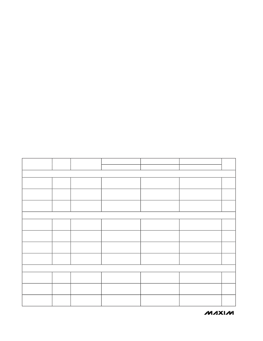
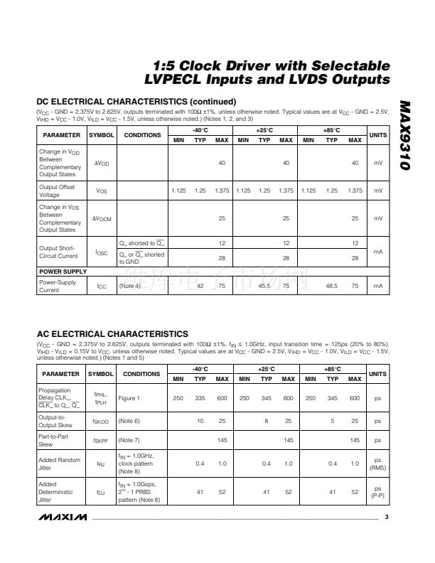
DC ELECTRICAL CHARACTERISTICS
(V
CC
- GND = 2.375V to 2.625V, outputs terminated with 100鈩?/div>
卤1%,
unless otherwise noted. Typical values are at V
CC
- GND = 2.5V,
V
IHD
= V
CC
- 1.0V, V
ILD
= V
CC
- 1.5V, unless otherwise noted.) (Notes 1, 2, and 3)
PARAMETER
SYMBOL
CONDITIONS
-40掳C
MIN
TYP
MAX
MIN
+25掳C
TYP
MAX
MIN
+85掳C
TYP
MAX
UNITS
SINGLE-ENDED INPUTS (CLKSEL,
EN)
Input High
Voltage
Input Low
Voltage
Input Current
V
IH
V
IL
I
IN
V
IH(MAX)
,
V
IL(MAX)
V
CC
-
1.165
V
CC
-
1.81
-150
V
CC
-
0.88
V
CC
-
1.475
+50
V
CC
-
1.165
V
CC
-
1.81
-150
V
CC
-
0.88
V
CC
-
1.475
+50
V
CC
-
1.165
V
CC
-
1.81
-150
V
CC
-
0.88
V
CC
-
1.475
+50
V
V
碌A
DIFFERENTIAL INPUTS (CLK_,
CLK_)
Differential Input
High Voltage
Differential Input
Low Voltage
Differential Input
Voltage
Input Current
OUTPUTS (Q_,
Q_)
Output High
Voltage
Output Low
Voltage
Differential
Output Voltage
V
OH
V
OL
V
OD
Figure 1
Figure 1
V
OH
- V
OL
,
Figure 1
0.9
250
350
450
1.6
0.9
250
350
450
1.6
0.9
250
350
450
1.6
V
V
mV
V
IHD
V
ILD
V
ID
I
IH
, I
IL
Figure 1
Figure 1
V
IHD
- V
ILD
CLK_, or
CLK_
=
V
IHD
or V
ILD
1.2
GND
0.095
-60
V
CC
V
CC
-
0.095
V
CC
+50
1.2
GND
0.095
-60
V
CC
V
CC
-
0.095
V
CC
+50
1.2
GND
0.095
-60
V
CC
V
CC
-
0.095
V
CC
+60
V
V
V
碌A
2
_______________________________________________________________________________________


 1
1
 2
2
 3
3
 4
4
 5
5
 6
6
 7
7
 8
8
 9
9
