- GND = 2.5V, outputs terminated with 100鈩?/div>
卤1%,
f
IN
= 1.0GHz, input transition time = 125ps (20% to 80%),V
IHD
= V
CC
- 1.0V,
V
ILD
= V
CC
- 1.5V, unless otherwise noted.)
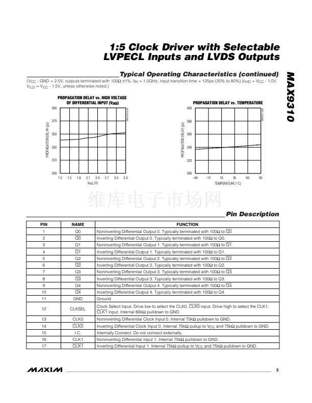
PROPAGATION DELAY vs. HIGH VOLTAGE
OF DIFFERENTIAL INPUT (V
IHD
)
MAX9310 toc04
PROPAGATION DELAY vs. TEMPERATURE
MAX9310 toc05
390
400
PROPAGATION DELAY (ps)
350
PROPAGATION DELAY (ps)
1.2
1.5
1.8
2.1
2.4
2.7
3.0
3.3
370
380
360
330
340
310
320
290
V
IHD
(V)
300
-40
-15
10
35
60
85
TEMPERATURE (掳C)
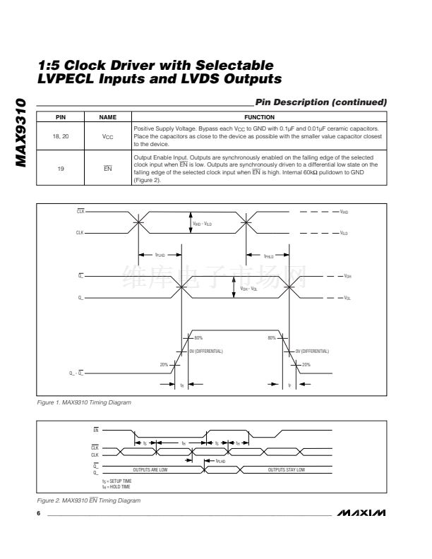
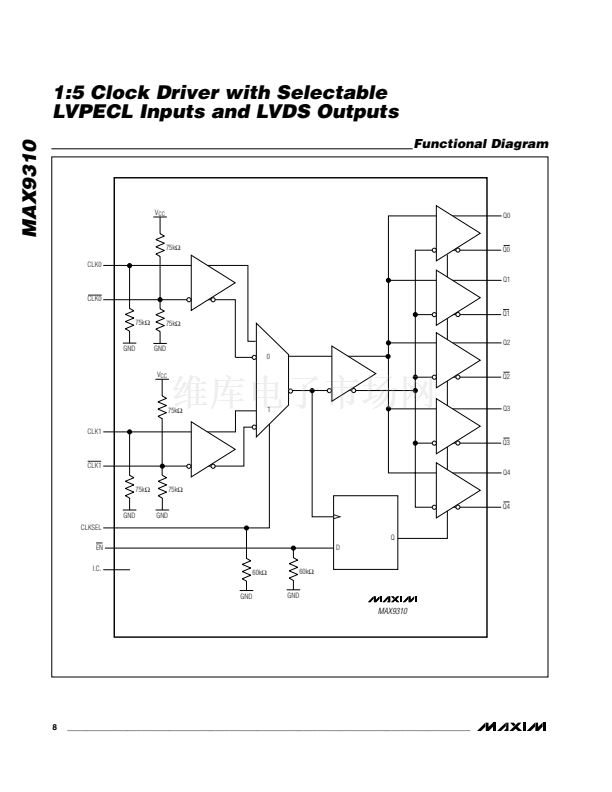
Pin Description
PIN
1
2
3
4
5
6
7
8
9
10
11
12
13
14
15
16
17
NAME
Q0
Q0
Q1
Q1
Q2
Q2
Q3
Q3
Q4
Q4
GND
CLKSEL
CLK0
CLK0
I.C.
CLK1
CLK1
FUNCTION
Noninverting Differential Output 0. Typically terminated with 100鈩?to
Q0.
Inverting Differential Output 0. Typically terminated with 100鈩?to Q0.
Noninverting Differential Output 1. Typically terminated with 100鈩?to
Q1.
Inverting Differential Output 1. Typically terminated with 100鈩?to Q1.
Noninverting Differential Output 2. Typically terminated with 100鈩?to
Q2.
Inverting Differential Output 2. Typically terminated with 100鈩?to Q2.
Noninverting Differential Output 3. Typically terminated with 100鈩?to
Q3.
Inverting Differential Output 3. Typically terminated with 100鈩?to Q3.
Noninverting Differential Output 4. Typically terminated with 100鈩?to
Q4.
Inverting Differential Output 4. Typically terminated with 100鈩?to Q4.
Ground
Clock Select Input. Drive low to select the CLK0,
CLK0
input. Drive high to select the CLK1,
CLK1
input. Internal 60k鈩?pulldown to GND.
Noninverting Differential Clock Input 0. Internal 75k鈩?pulldown to GND.
Inverting Differential Clock Input 0. Internal 75k鈩?pullup to V
CC
and 75k鈩?pulldown to GND.
Internally Connect. Do not connect externally.
Noninverting Differential Input 1. Internal 75k鈩?pulldown to GND.
Inverting Differential Input 1. Internal 75k鈩?pullup to V
CC
and 75k鈩?pulldown to GND.
_______________________________________________________________________________________
5


 1
1
 2
2
 3
3
 4
4
 5
5
 6
6
 7
7
 8
8
 9
9
