1:5 Clock Driver with Selectable
LVPECL Inputs and LVDS Outputs
MAX9310
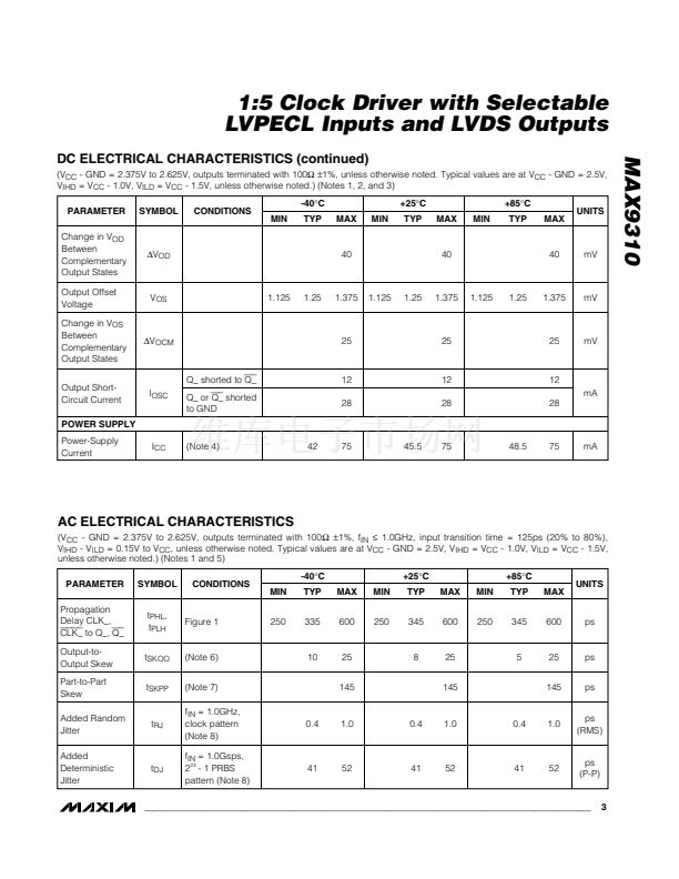
Pin Description (continued)
PIN
18, 20
NAME
V
CC
FUNCTION
Positive Supply Voltage. Bypass each V
CC
to GND with 0.1碌F and 0.01碌F ceramic capacitors.
Place the capacitors as close to the device as possible with the smaller value capacitor closest
to the device.
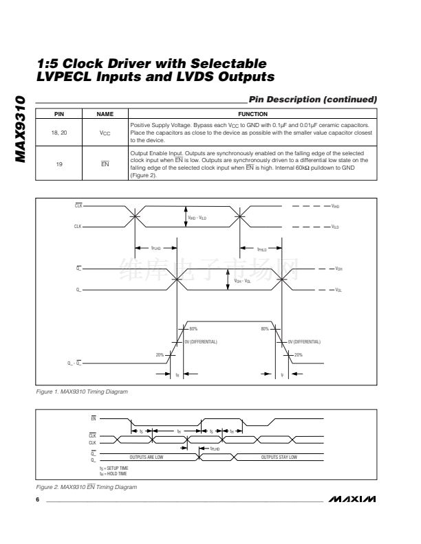
Output Enable Input. Outputs are synchronously enabled on the falling edge of the selected
clock input when
EN
is low. Outputs are synchronously driven to a differential low state on the
falling edge of the selected clock input when
EN
is high. Internal 60k鈩?pulldown to GND
(Figure 2).
19
EN
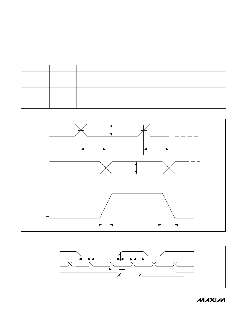
CLK
V
IHD
- V
ILD
CLK
V
IHD
V
ILD
t
PLHD
t
PHLD
Q_
V
OH
- V
OL
Q_
V
OH
V
OL
80%
0V (DIFFERENTIAL)
20%
Q_ - Q_
t
R
80%
0V (DIFFERENTIAL)
20%
t
F
Figure 1. MAX9310 Timing Diagram
EN
t
S
t
H
t
S
t
H
CLK
CLK
Q_
Q_
t
S
= SETUP TIME
t
H
= HOLD TIME
t
PLHD
OUTPUTS ARE LOW
OUTPUTS STAY LOW
Figure 2. MAX9310
EN
Timing Diagram
6
_______________________________________________________________________________________


 1
1
 2
2
 3
3
 4
4
 5
5
 6
6
 7
7
 8
8
 9
9
