Ultra-Low-Power, Open-Drain,
Single/Dual-Supply Comparators
MAX971鈥揗AX974/MAX981鈥揗AX984
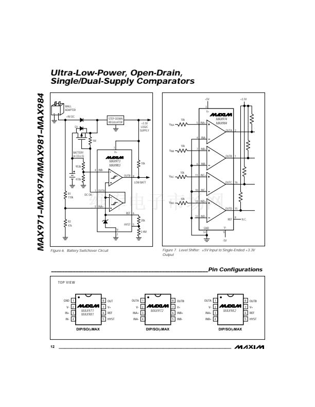
_______________Detailed Description
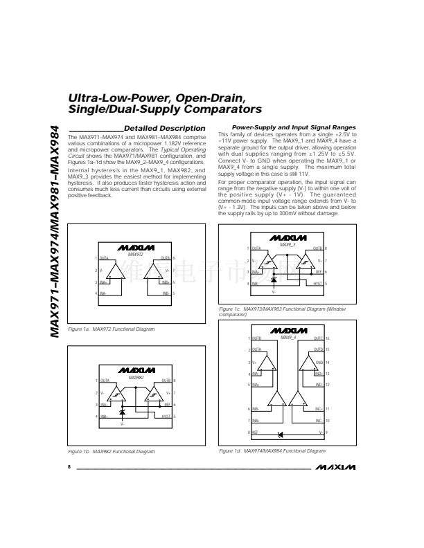
The MAX971鈥揗AX974 and MAX981鈥揗AX984 comprise
various combinations of a micropower 1.182V reference
and micropower comparators. The
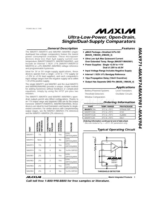
Typical Operating
Circuit
shows the MAX971/MAX981 configuration, and
Figures 1a鈥?d show the MAX9_2鈥揗AX9_4 configurations.
Internal hysteresis in the MAX9_1, MAX982, and
MAX9_3 provides the easiest method for implementing
hysteresis. It also produces faster hysteresis action and
consumes much less current than circuits using external
positive feedback.
Power-Supply and Input Signal Ranges
This family of devices operates from a single +2.5V to
+11V power supply. The MAX9_1 and MAX9_4 have a
separate ground for the output driver, allowing operation
with dual supplies ranging from 卤1.25V to 卤5.5V.
Connect V- to GND when operating the MAX9_1 or
MAX9_4 from a single supply. The maximum total
supply voltage in this case is still 11V.
For proper comparator operation, the input signal can
range from the negative supply (V-) to within one volt of
the positive supply (V+ - 1V). The guaranteed
common-mode input voltage range extends from V- to
(V+ - 1.3V). The inputs can be taken above and below
the supply rails by up to 300mV without damage.
1 OUTA
1 OUTA
2 V-
3 INA+
4 INA-
MAX9_3
OUTB 8
V+ 7
REF 6
HYST 5
MAX972
OUTB 8
V+ 7
INB+ 6
INB- 5
2 V-
3 INA+
4 INB-
V-
Figure 1c. MAX973/MAX983 Functional Diagram (Window
Comparator)
Figure 1a. MAX972 Functional Diagram
1 OUTB
2 OUTA
3 V+
4 INA-
OUTB 8
5 INA+
2 V-
3 INA+
4 INB+
V-
V+ 7
REF 6
6 INB-
HYST 5
7 INB+
8 REF
INC- 10
V- 9
INC+ 11
IND- 12
MAX9_4
OUTC 16
OUTD 15
GND 14
IND+ 13
1 OUTA
MAX982
Figure 1b. MAX982 Functional Diagram
8
Figure 1d. MAX974/MAX984 Functional Diagram
_______________________________________________________________________________________


 1
1
 2
2
 3
3
 4
4
 5
5
 6
6
 7
7
 8
8
 9
9
 10
10
 11
11
 12
12
 13
13
 14
14
 15
15
 16
16
