Ultra-Low-Power, Open-Drain,
Single/Dual-Supply Comparators
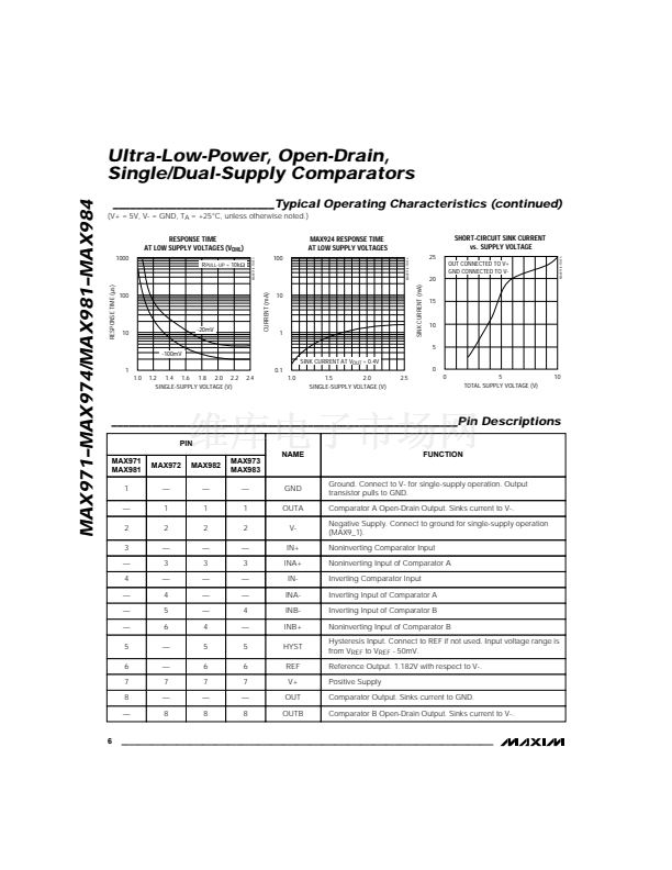
The negative supply does not affect the output sink
current. The positive supply provides gate drive for the
output N-channel MOSFET and heavily influences the
output current capability, especially at low supply
voltages (see
Typical Operating Characteristics
section).
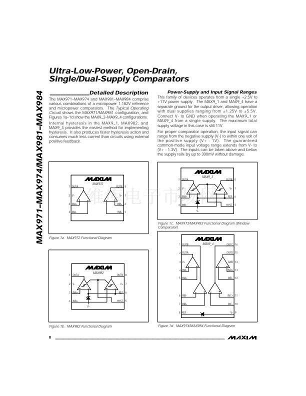
The MAX9_2 and MAX9_3 have no GND pin, and their
outputs sink current to V-.
MAX971鈥揗AX974/MAX981鈥揗AX984
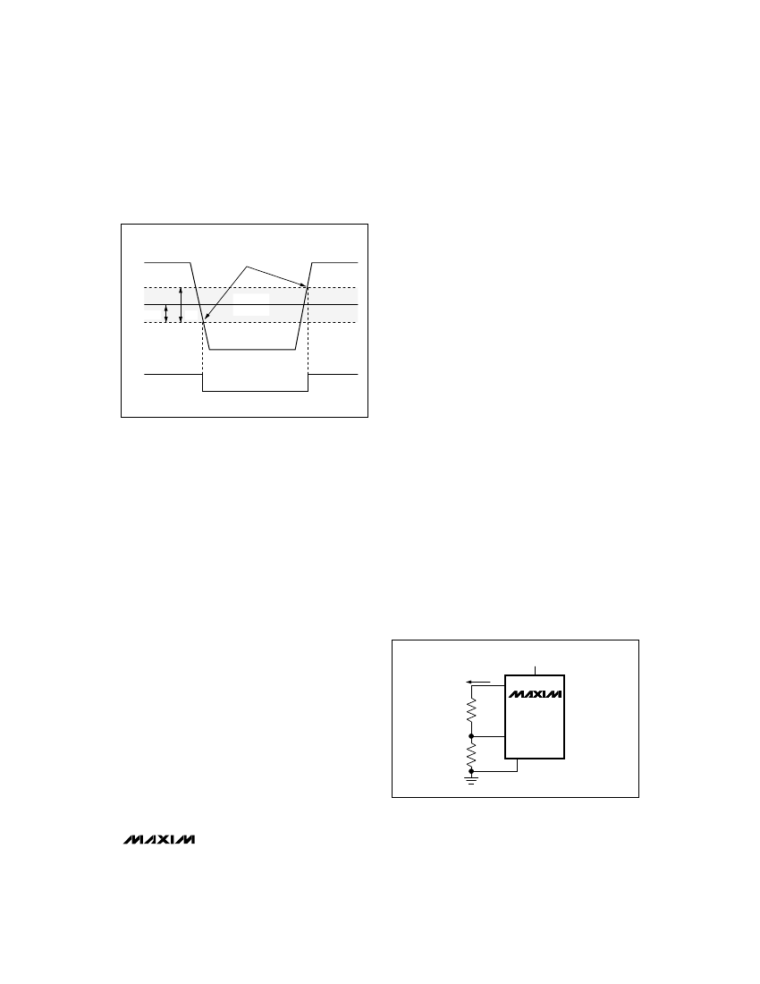
IN+
THRESHOLDS
IN-
V
REF
- V
HYST
HYSTERESIS
V
HB
BAND
Voltage Reference
The internal bandgap voltage reference has an output
of 1.182V above V-. Note that the REF voltage is
referenced to V-, not to GND. Its accuracy is 卤1%
(MAX971/MAX973/MAX974) or 卤2% (MAX981鈥揗AX984)
in the 0掳C to +70掳C range. The REF output is typically
capable of sourcing 25碌A and sinking 15碌A. Do not
bypass the REF output.
OUT
Noise Considerations
Figure 2. Threshold Hysteresis Band
Low-Voltage Operation: V+ = 1V (MAX9_4 Only)
The guaranteed minimum operating voltage is 2.5V (or
卤1.25V). As the total supply voltage falls below 2.5V,
performance degrades and the supply current falls.
The reference will not function below about 2.2V,
although the comparators will continue to operate with a
total supply voltage as low as 1V. While the MAX9_4
has comparators that may be used at supply voltages
below 2V, the MAX9_1/MAX9_2/MAX9_3 may not be
used with supply voltages below 2.5V.
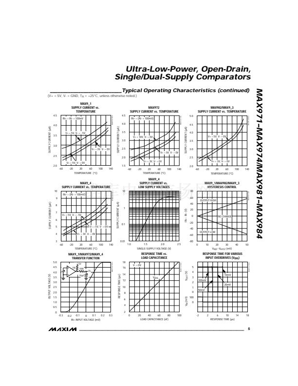
At low supply voltages, the comparators鈥?output sink
capability is reduced and the propagation delay
increases (see
Typical Operating Characteristics).
The
useful input voltage range extends from the negative
supply to a little under 1V below the positive supply,
which is slightly closer to the positive rail than when the
device operates from higher supply voltages. Test your
prototype over the full temperature and supply-voltage
range if you anticipate operation below 2.5V.
Although the comparators have a very high gain, useful
gain is limited by noise. This is shown in the Transfer
Function graph (see
Typical Operating Characteristics).
As the input voltage approaches the comparator鈥檚
offset, the output begins to bounce back and forth; this
peaks when V
IN
= V
OS
. (The lowpass filter shown on the
graph averages out the bouncing, making the transfer
function easy to observe.) Consequently, the
comparator has an effective wideband peak-to-peak
noise of around 300碌V. The voltage reference has
peak-to-peak noise approaching 1mV. Thus, when a
comparator is used with the reference, the combined
peak-to-peak noise is about 1mV. This, of course, is
much higher than the RMS noise of the individual
components. Take care in your layout to avoid
capacitive coupling from any output to the reference
pin. Crosstalk can significantly increase the actual
noise of the reference.
Comparator Output
With 100mV of overdrive, propagation delay is typically
3碌s. The
Typical Operating Characteristics
show the
propagation delay for various overdrive levels. The
open-drain outputs are intended for wire-ORed and
level-shifting applications. The maximum output
voltage is 11V above V-, and may be applied even
when no supply voltage is present (V+ = V-).
The MAX9_1 and MAX9_4 outputs sink current to GND,
making these devices ideal for bipolar to single-ended
conversion and level-shifting applications.
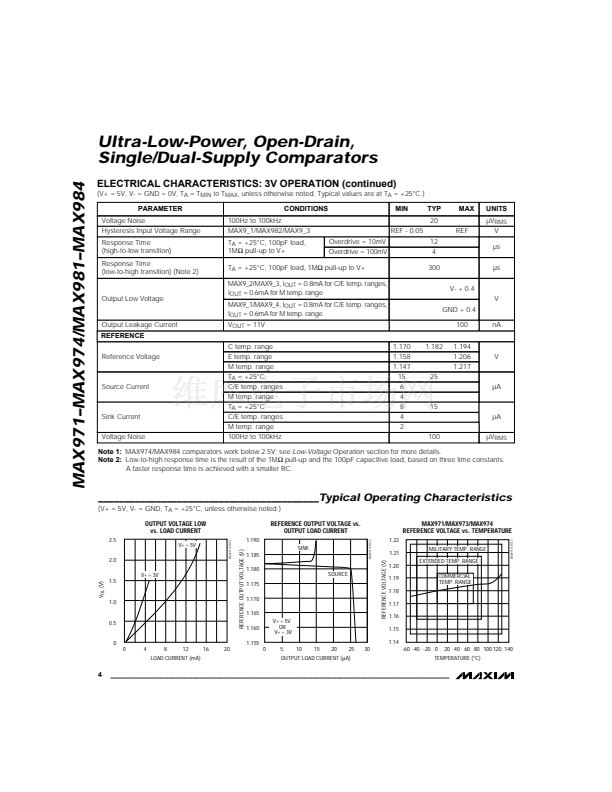
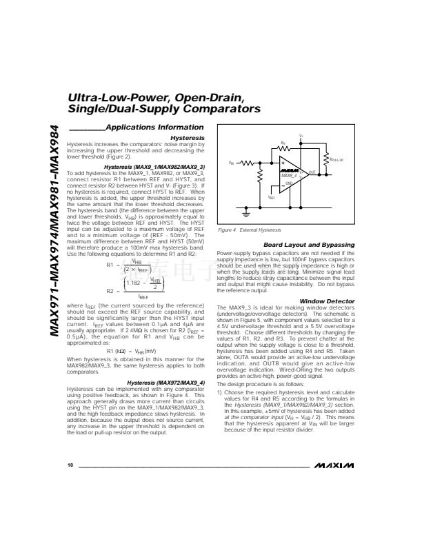
R1
I
REF
6
REF
2.5V TO 11V
7
V+
MAX9_1
MAX982
MAX9_3
5
HYST
V-
2
R2
Figure 3. Programming the HYST Pin
_______________________________________________________________________________________
9


 1
1
 2
2
 3
3
 4
4
 5
5
 6
6
 7
7
 8
8
 9
9
 10
10
 11
11
 12
12
 13
13
 14
14
 15
15
 16
16
