Philips Semiconductors
Preliminary speci铿乧ation
Full bridge vertical de铿俥ction output circuit
in LVDMOS
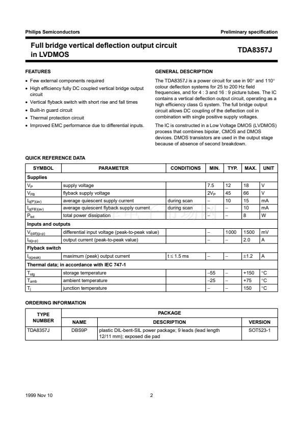
LIMITING VALUES
In accordance with the Absolute Maximum Rating System (IEC 134).
SYMBOL
V
P
V
FB
V
n
supply voltage
铿倅back supply voltage
DC voltage
pin OUTA
pin OUTB
pins INA, INB, GUARD and FEEDB
I
n
DC current
pins OUTA and OUTB
pins OUTA and OUTB
pins INA, INB, GUARD and FEEDB
I
lu
latch-up current
current into any pin; pin voltage
is 1.5
脳
V
P
; note 2
current out of any pin; pin voltage
is
鈭?.5 脳
V
P
; note 2
V
es
P
tot
T
stg
T
amb
T
j
Notes
1. When the voltage at pin OUTA supersedes 70 V the circuit will limit the voltage.
2. At T
j(max)
.
3. Equivalent to 200 pF capacitance discharge through a 0
鈩?/div>
resistor.
4. Equivalent to 100 pF capacitance discharge through a 1.5 k鈩?resistor.
5. Internally limited by thermal protection at T
j
鈮?/div>
170
掳C.
THERMAL CHARACTERISTICS
In accordance with IEC 747-1.
SYMBOL
R
th(j-c)
R
th(j-a)
PARAMETER
thermal resistance from junction to case
thermal resistance from junction to ambient
in free air
CONDITIONS
MIN.
鈭?/div>
鈭?/div>
TYP.
鈭?/div>
鈭?/div>
electrostatic handling voltage
total power dissipation
storage temperature
ambient temperature
junction temperature
note 5
machine model; note 3
human body model; note 4
during scan (p-p)
at 铿倅back (peak); t
鈮?/div>
1.5 ms
鈭?/div>
鈭?/div>
鈭?0
鈭?/div>
鈭?00
鈭?00
鈭?/div>
鈭?5
鈭?5
鈭?/div>
note 1
鈭?/div>
鈭?/div>
鈭?.5
PARAMETER
CONDITIONS
MIN.
鈭?/div>
鈭?/div>
TDA8357J
MAX.
18
68
68
V
P
V
P
2.0
卤1.2
+20
+200
鈭?/div>
+300
8
+150
+75
150
UNIT
V
V
V
V
V
A
A
mA
mA
mA
V
W
掳C
掳C
掳C
鈭?000
+2000 V
MAX.
6
65
UNIT
K/W
K/W
1999 Nov 10
5
TDA8357J相关型号PDF文件下载
-
型号
版本
描述
厂商
下载
-
英文版
Octuple 6-bit DACs with I2C-bus
PHILIPS
-
英文版
Octuple 6-bit DACs with I2C-bus
PHILIPS [N...
-
英文版
Smart card interface
PHILIPS
-
英文版
Smart card interface
PHILIPS [N...
-
英文版
Smart card interface
PHILIPS
-
英文版
Smart card interface
PHILIPS [N...
-
英文版
IC card interface
PHILIPS
-
英文版
IC card interface
PHILIPS [N...
-
英文版
IC card interface
PHILIPS
-
英文版
IC card interface
PHILIPS [N...
-
英文版
Low-power smart card coupler
PHILIPS
-
英文版
Low-power smart card coupler
PHILIPS [N...
-
英文版
Multiprotocol IC Card coupler
Philips
-
英文版
Dual multiprotocol smart card
Philips
-
英文版
Low power mixers/oscillators for satellite tuners
PHILIPS
-
英文版
Low power mixers/oscillators for satellite tuners
PHILIPS [N...
-
英文版
IF amplifier for satellite TV receivers
PHILIPS
-
英文版
IF amplifier for satellite TV receivers
PHILIPS [N...
-
英文版
Dual smart card interface
PHILIPS
-
英文版
Dual smart card interface
PHILIPS [N...


 1
1
 2
2
 3
3
 4
4
 5
5
 6
6
 7
7
 8
8
 9
9
 10
10
 11
11
 12
12
 13
13
 14
14
 15
15
 16
16
