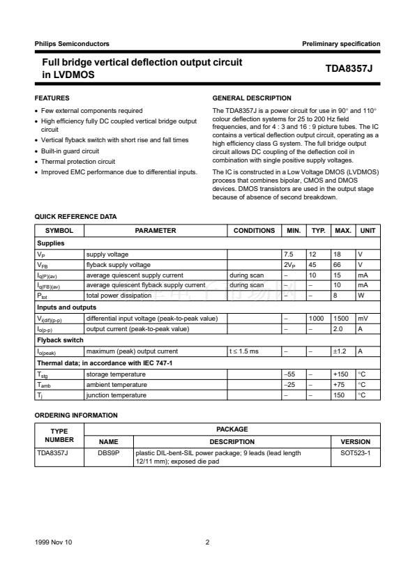
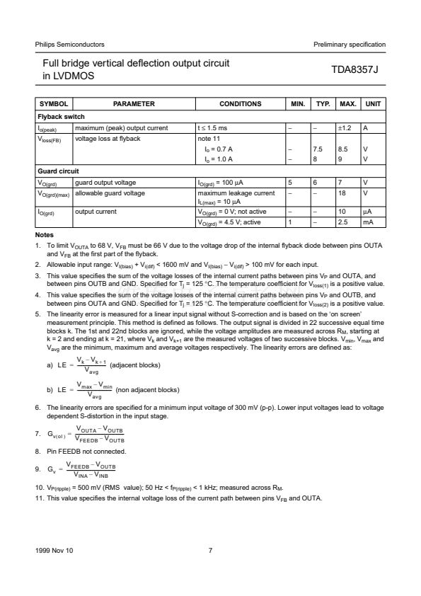
MIN.
TYP.
MAX.
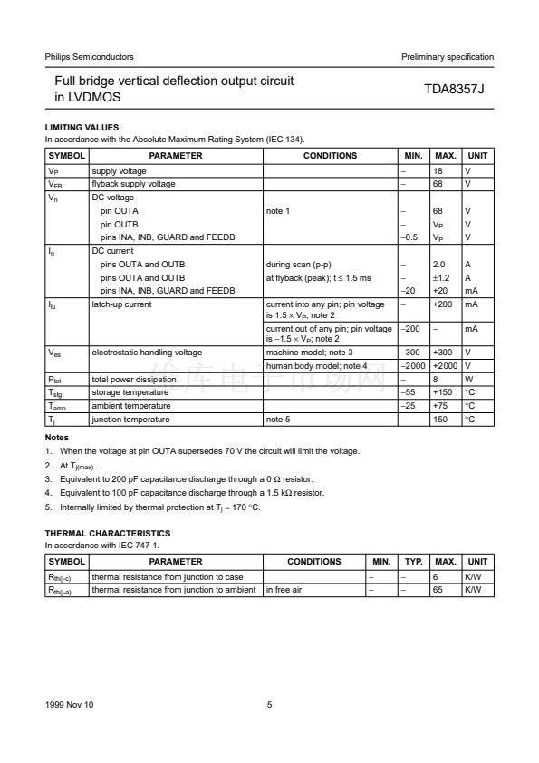
1. To limit V
must be 66 V due to the voltage drop of the internal flyback diode between pins OUTA
at the first part of the flyback.
2. Allowable input range: V
鈭?/div>
V
i(dif)
> 100 mV for each input.
3. This value specifies the sum of the voltage losses of the internal current paths between pins V
P
and OUTA, and
between pins OUTB and GND. Specified for T
j
= 125
掳C.
The temperature coefficient for V
loss(1)
is a positive value.
4. This value specifies the sum of the voltage losses of the internal current paths between pins V
P
and OUTB, and
between pins OUTA and GND. Specified for T
j
= 125
掳C.
The temperature coefficient for V
loss(2)
is a positive value.
5. The linearity error is measured for a linear input signal without S-correction and is based on the 鈥榦n screen鈥?/div>
measurement principle. This method is defined as follows. The output signal is divided in 22 successive equal time
blocks k. The 1st and 22nd blocks are ignored, while the voltage amplitudes are measured across R
M
, starting at
k = 2 and ending at k = 21, where V
k
and V
k+1
are the measured voltages of two successive blocks. V
min
, V
max
and
V
avg
are the minimum, maximum and average voltages respectively. The linearity errors are defined as:
V
k
鈥?/div>
V
k
+
1
a) LE
=
------------------------- (adjacent blocks)
-
V
avg
V
max
鈥?/div>
V
min
b) LE
=
------------------------------ (non adjacent blocks)
-
V
avg
6. The linearity errors are specified for a minimum input voltage of 300 mV (p-p). Lower input voltages lead to voltage
dependent S-distortion in the input stage.
7.
V
OUTA
鈥?/div>
V
OUTB
G
v
(
ol
)
=
-------------------------------------------
-
V
FEEDB
鈥?/div>
V
OUTB
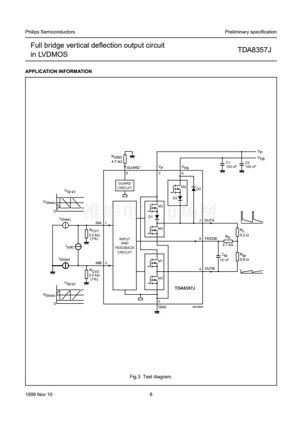
8. Pin FEEDB not connected.
9.
V
FEEDB
鈥?/div>
V
OUTB
G
v
=
-------------------------------------------
-
V
INA
鈥?/div>
V
INB
10. V
P(ripple)
= 500 mV (RMS value); 50 Hz < f
P(ripple)
< 1 kHz; measured across R
M
.
11. This value specifies the internal voltage loss of the current path between pins V
FB
and OUTA.
1999 Nov 10
7
TDA8357J相关型号PDF文件下载
-
型号
版本
描述
厂商
下载
-
英文版
Octuple 6-bit DACs with I2C-bus
PHILIPS
-
英文版
Octuple 6-bit DACs with I2C-bus
PHILIPS [N...
-
英文版
Smart card interface
PHILIPS
-
英文版
Smart card interface
PHILIPS [N...
-
英文版
Smart card interface
PHILIPS
-
英文版
Smart card interface
PHILIPS [N...
-
英文版
IC card interface
PHILIPS
-
英文版
IC card interface
PHILIPS [N...
-
英文版
IC card interface
PHILIPS
-
英文版
IC card interface
PHILIPS [N...
-
英文版
Low-power smart card coupler
PHILIPS
-
英文版
Low-power smart card coupler
PHILIPS [N...
-
英文版
Multiprotocol IC Card coupler
Philips
-
英文版
Dual multiprotocol smart card
Philips
-
英文版
Low power mixers/oscillators for satellite tuners
PHILIPS
-
英文版
Low power mixers/oscillators for satellite tuners
PHILIPS [N...
-
英文版
IF amplifier for satellite TV receivers
PHILIPS
-
英文版
IF amplifier for satellite TV receivers
PHILIPS [N...
-
英文版
Dual smart card interface
PHILIPS
-
英文版
Dual smart card interface
PHILIPS [N...


 1
1
 2
2
 3
3
 4
4
 5
5
 6
6
 7
7
 8
8
 9
9
 10
10
 11
11
 12
12
 13
13
 14
14
 15
15
 16
16
