www.ti.com
TPS76815Q, TPS76818Q, TPS76825Q
TPS76827Q, TPS76828Q, TPS76830Q
TPS76833Q, TPS76850Q, TPS76801Q
SLVS211J 鈥?JUNE 1999 鈥?REVISED OCTOBER 2004
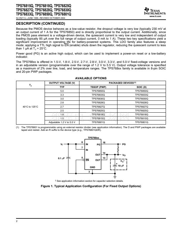
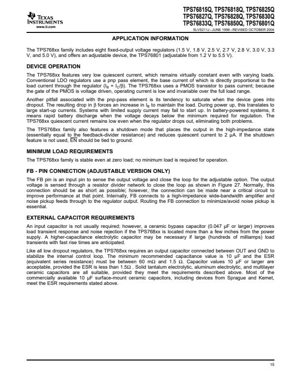
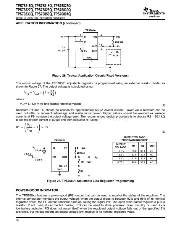
APPLICATION INFORMATION (continued)
REGULATOR PROTECTION
The TPS768xx PMOS-pass transistor has a built-in back diode that conducts reverse currents when the input
voltage drops below the output voltage (e.g., during power down). Current is conducted from the output to the
input and is not internally limited. When extended reverse voltage is anticipated, external limiting may be
appropriate.
The TPS768xx also features internal current limiting and thermal protection. During normal operation, the
TPS768xx limits output current to approximately 1.7 A. When current limiting engages, the output voltage scales
back linearly until the overcurrent condition ends. While current limiting is designed to prevent gross device
failure, care should be taken not to exceed the power dissipation ratings of the package. If the temperature of the
device exceeds 150掳C (typ), thermal-protection circuitry shuts it down. Once the device has cooled below 130掳C
(typ), regulator operation resumes.
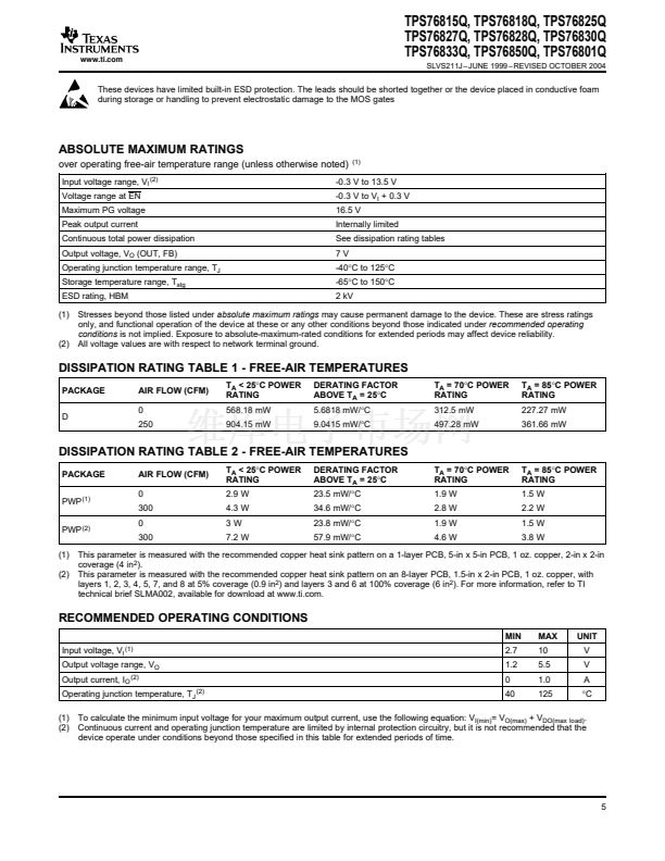
POWER DISSIPATION AND JUNCTION TEMPERATURE
Specified regulator operation is assured to a junction temperature of 125掳C; the maximum junction temperature
should be restricted to 125掳C under normal operating conditions. This restriction limits the power dissipation the
regulator can handle in any given application. To ensure the junction temperature is within acceptable limits,
calculate the maximum allowable dissipation, P
D(max)
, and the actual dissipation, P
D
, which must be less than or
equal to P
D(max)
.
The maximum-power-dissipation limit is determined using the following equation:
T max
*
T
A
P
+
J
D(max)
R
qJA
where:
T
J
max is the maximum allowable junction temperature.
R
胃JA
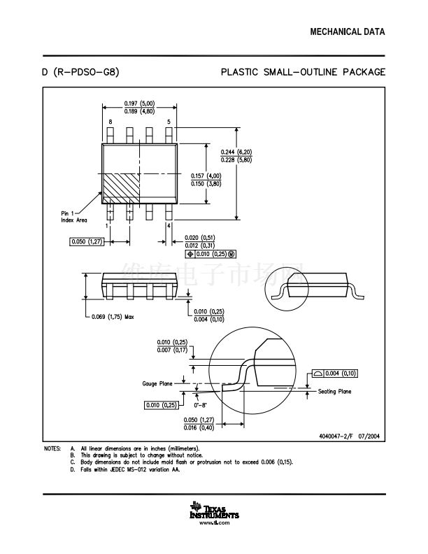
is the thermal resistance junction-to-ambient for the package, i.e., 172掳C/W for the 8-terminal
SOIC and 32.6掳C/W for the 20-terminal PWP with no airflow.
T
A
is the ambient temperature.
(3)
The regulator dissipation is calculated using:
P
D
+
V
*
V
I
O
I
O
(4)
Power dissipation resulting from quiescent current is negligible. Excessive power dissipation will trigger the
thermal protection circuit.
17


 1
1
 2
2
 3
3
 4
4
 5
5
 6
6
 7
7
 8
8
 9
9
 10
10
 11
11
 12
12
 13
13
 14
14
 15
15
 16
16
 17
17
 18
18
 19
19
 20
20
 21
21
 22
22
