www.ti.com
TPS76815Q, TPS76818Q, TPS76825Q
TPS76827Q, TPS76828Q, TPS76830Q
TPS76833Q, TPS76850Q, TPS76801Q
SLVS211J 鈥?JUNE 1999 鈥?REVISED OCTOBER 2004
These devices have limited built-in ESD protection. The leads should be shorted together or the device placed in conductive foam
during storage or handling to prevent electrostatic damage to the MOS gates
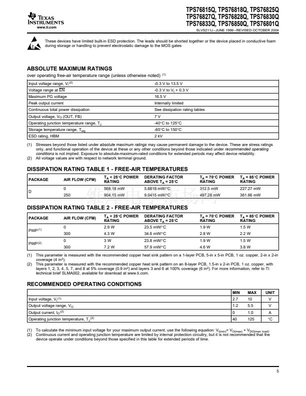
ABSOLUTE MAXIMUM RATINGS
over operating free-air temperature range (unless otherwise noted)
Input voltage range, V
I (2)
Voltage range at EN
Maximum PG voltage
Peak output current
Continuous total power dissipation
Output voltage, V
O
(OUT, FB)
Operating junction temperature range, T
J
Storage temperature range, T
stg
ESD rating, HBM
(1)
(2)
(1)
-0.3 V to 13.5 V
-0.3 V to V
I
+ 0.3 V
16.5 V
Internally limited
See dissipation rating tables
7V
-40掳C to 125掳C
-65掳C to 150掳C
2 kV
Stresses beyond those listed under
absolute maximum ratings
may cause permanent damage to the device. These are stress ratings
only, and functional operation of the device at these or any other conditions beyond those indicated under
recommended operating
conditions
is not implied. Exposure to absolute-maximum-rated conditions for extended periods may affect device reliability.
All voltage values are with respect to network terminal ground.
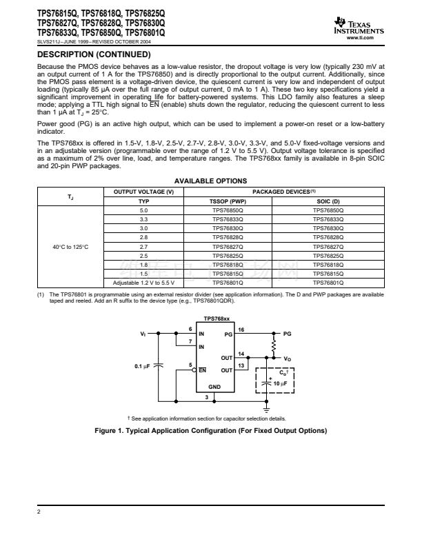
DISSIPATION RATING TABLE 1 - FREE-AIR TEMPERATURES
PACKAGE
D
AIR FLOW (CFM)
0
250
T
A
< 25掳C POWER
RATING
568.18 mW
904.15 mW
DERATING FACTOR
ABOVE T
A
= 25掳C
5.6818 mW/掳C
9.0415 mW/掳C
T
A
= 70掳C POWER
RATING
312.5 mW
497.28 mW
T
A
= 85掳C POWER
RATING
227.27 mW
361.66 mW
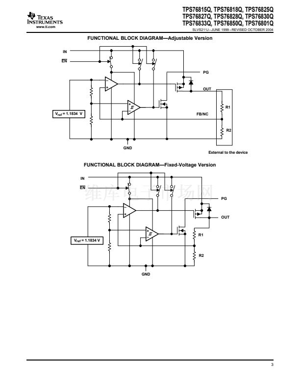
DISSIPATION RATING TABLE 2 - FREE-AIR TEMPERATURES
PACKAGE
PWP
(1)
PWP
(2)
(1)
(2)
AIR FLOW (CFM)
0
300
0
300
T
A
< 25掳C POWER
RATING
2.9 W
4.3 W
3W
7.2 W
DERATING FACTOR
ABOVE T
A
= 25掳C
23.5 mW/掳C
34.6 mW/掳C
23.8 mW/掳C
57.9 mW/掳C
T
A
= 70掳C POWER
RATING
1.9 W
2.8 W
1.9 W
4.6 W
T
A
= 85掳C POWER
RATING
1.5 W
2.2 W
1.5 W
3.8 W
This parameter is measured with the recommended copper heat sink pattern on a 1-layer PCB, 5-in x 5-in PCB, 1 oz. copper, 2-in x 2-in
coverage (4 in
2
).
This parameter is measured with the recommended copper heat sink pattern on an 8-layer PCB, 1.5-in x 2-in PCB, 1 oz. copper, with
layers 1, 2, 3, 4, 5, 7, and 8 at 5% coverage (0.9 in
2
) and layers 3 and 6 at 100% coverage (6 in
2
). For more information, refer to TI
technical brief SLMA002, available for download at www.ti.com.
RECOMMENDED OPERATING CONDITIONS
MIN
Input voltage, V
I
(1)
MAX
10
5.5
1.0
125
UNIT
V
V
A
掳C
2.7
1.2
0
40
Output voltage range, V
O
Output current, I
O (2)
Operating junction temperature, T
J (2)
(1)
(2)
To calculate the minimum input voltage for your maximum output current, use the following equation: V
I(min)
= V
O(max)
+ V
DO(max load)
.
Continuous current and operating junction temperature are limited by internal protection circuitry, but it is not recommended that the
device operate under conditions beyond those specified in this table for extended periods of time.
5


 1
1
 2
2
 3
3
 4
4
 5
5
 6
6
 7
7
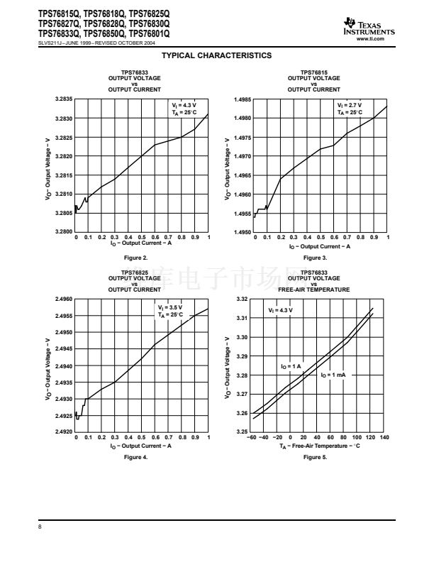 8
8
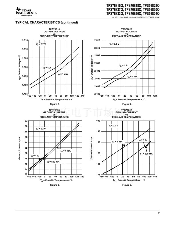 9
9
 10
10
 11
11
 12
12
 13
13
 14
14
 15
15
 16
16
 17
17
 18
18
 19
19
 20
20
 21
21
 22
22
