TPS76815Q, TPS76818Q, TPS76825Q
TPS76827Q, TPS76828Q, TPS76830Q
TPS76833Q, TPS76850Q, TPS76801Q
SLVS211J 鈥?JUNE 1999 鈥?REVISED OCTOBER 2004
www.ti.com
DESCRIPTION (CONTINUED)
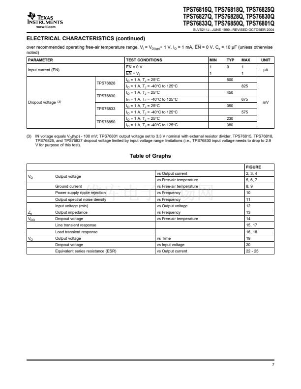
Because the PMOS device behaves as a low-value resistor, the dropout voltage is very low (typically 230 mV at
an output current of 1 A for the TPS76850) and is directly proportional to the output current. Additionally, since
the PMOS pass element is a voltage-driven device, the quiescent current is very low and independent of output
loading (typically 85 碌A over the full range of output current, 0 mA to 1 A). These two key specifications yield a
significant improvement in operating life for battery-powered systems. This LDO family also features a sleep
mode; applying a TTL high signal to EN (enable) shuts down the regulator, reducing the quiescent current to less
than 1 碌A at T
J
= 25掳C.
Power good (PG) is an active high output, which can be used to implement a power-on reset or a low-battery
indicator.
The TPS768xx is offered in 1.5-V, 1.8-V, 2.5-V, 2.7-V, 2.8-V, 3.0-V, 3.3-V, and 5.0-V fixed-voltage versions and
in an adjustable version (programmable over the range of 1.2 V to 5.5 V). Output voltage tolerance is specified
as a maximum of 2% over line, load, and temperature ranges. The TPS768xx family is available in 8-pin SOIC
and 20-pin PWP packages.
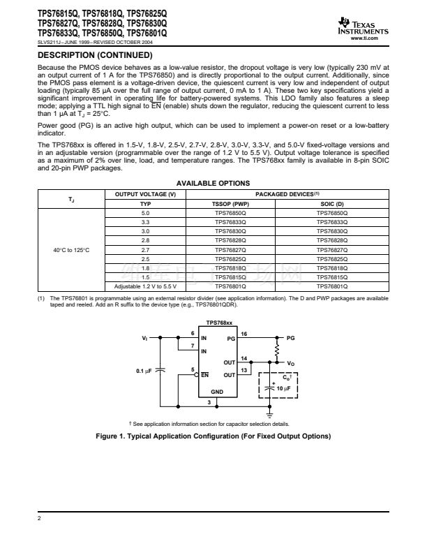
AVAILABLE OPTIONS
T
J
OUTPUT VOLTAGE (V)
TYP
5.0
3.3
3.0
2.8
40掳C to 125掳C
2.7
2.5
1.8
1.5
Adjustable 1.2 V to 5.5 V
(1)
TSSOP (PWP)
TPS76850Q
TPS76833Q
TPS76830Q
TPS76828Q
TPS76827Q
TPS76825Q
TPS76818Q
TPS76815Q
TPS76801Q
PACKAGED DEVICES
(1)
SOIC (D)
TPS76850Q
TPS76833Q
TPS76830Q
TPS76828Q
TPS76827Q
TPS76825Q
TPS76818Q
TPS76815Q
TPS76801Q
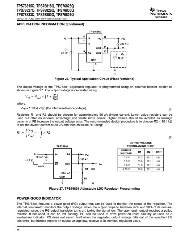
The TPS76801 is programmable using an external resistor divider (see application information). The D and PWP packages are available
taped and reeled. Add an R suffix to the device type (e.g., TPS76801QDR).
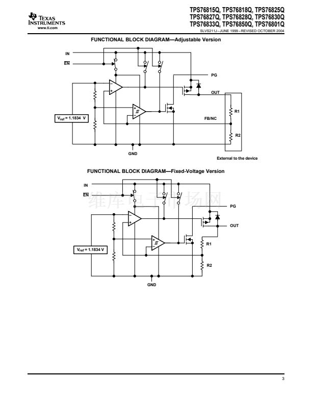
TPS768xx
V
I
6
7
IN
OUT
0.1
碌F
5
EN
GND
3
OUT
14
13
+
C
o
鈥?/div>
10
碌F
V
O
IN
PG
16
PG
鈥?/div>
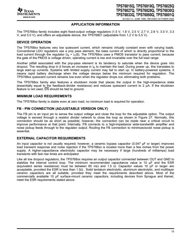
See application information section for capacitor selection details.
Figure 1. Typical Application Configuration (For Fixed Output Options)
2


 1
1
 2
2
 3
3
 4
4
 5
5
 6
6
 7
7
 8
8
 9
9
 10
10
 11
11
 12
12
 13
13
 14
14
 15
15
 16
16
 17
17
 18
18
 19
19
 20
20
 21
21
 22
22
