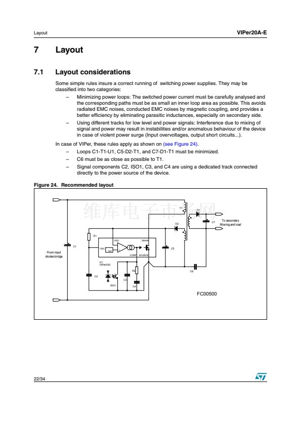
Some simple rules insure a correct running of switching power supplies. They may be
鈥?/div>
Minimizing power loops: The switched power current must be carefully analysed and
the corresponding paths must be as small an inner loop area as possible. This avoids
radiated EMC noises, conducted EMC noises by magnetic coupling, and provides a
better efficiency by eliminating parasitic inductances, especially on secondary side.
Using different tracks for low level and power signals: Interference due to mixing of
signal and power may result in instabilities and/or anomalous behaviour of the device
in case of violent power surge (Input overvoltages, output short circuits...).
Loops C1-T1-U1, C5-D2-T1, and C7-D1-T1 must be minimized.
C6 must be as close as possible to T1.
Signal components C2, ISO1, C3, and C4 are using a dedicated track connected
directly to the power source of the device.
鈥?/div>
In case of VIPer, these rules apply as shown on
(see Figure 24).
鈥?/div>
鈥?/div>
鈥?/div>
Figure 24. Recommended layout
T1
D1
D2
C7
To secondary
filtering and load
R1
VDD
DRAIN
C1
-
OSC
13V
+
COMP
SOURCE
C5
From input
diodes bridge
U1
VIPerXX0
R2
C2
C3
ISO1
C4
C6
FC00500
22/34


 1
1
 2
2
 3
3
 4
4
 5
5
 6
6
 7
7
 8
8
 9
9
 10
10
 11
11
 12
12
 13
13
 14
14
 15
15
 16
16
 17
17
 18
18
 19
19
 20
20
 21
21
 22
22
 23
23
 24
24
 25
25
 26
26
 27
27
 28
28
 29
29
 30
30
 31
31
 32
32
 33
33
 34
34
