基于PCF8811 LCD驱动方案
出处:NXP 发布于:2011-08-18 11:16:50
NXP (恩智浦半导体)是一家新近独立的半导体公司,由飞利浦公司创立,已拥有五十年的悠久历史,主要提供工程师与设计人员各种半导体产品与软件,为移动通信、消费类电子、安全应用、非接触式付费与连线,以及车内娱乐与网络等产品带来更优质的感知体验。PCF8811是由NXP 公司推出的,具有8位并行接口,3/4路SPI和高速I2C总线,适合于以电池为能源的系统,主要用于汽车显示器,通信设备,手提仪表和POS终端。
LCD对于许多的用户而言可能是一个并不算新鲜的名词了,不过这种技术存在的历史可能远远超过了我们的想像 -早在19世纪末,奥地利植物学家就发现了液晶,即液态的晶体,也就是说一种物质同时具备了液体的流动性和类似晶体的某种排列特性。在电场的作用下,液晶分子的排列会产生变化。从而影响到它的光学性质,这种现象叫做电光效应。利用液晶的电光效应,英国科学家在上世纪制造了块液晶显示器即LCD.今天的液晶显示器中广泛采用的是定线状液晶,如果我们微观去看它,会发现它特象棉花棒。与传统的CRT相比,LCD不但体积小,厚度薄(目前14.1英寸的整机厚度可做到只有5厘米),重量轻、耗能少(1到10 微瓦/平方厘米)、工作电压低(1.5到6V)且无辐射,无闪烁并能直接与CMOS集成电路匹配。
PCF8811:80 x 128 pixels matrix LCD driver
The PCF8811 is a low-power CMOS1 LCD controller and driver, designed to drive a graphic display of 80 rows and 128 columns or a graphic display of 79 rows and 128 columns and an icon row of 128 symbols. All necessary functions for the display are provided in a single chip, including on-chip generation of the LCD supply and bias voltages, resulting in a minimum of external components and low power consumption. The PCF8811 can interface microcontrollers via a parallel bus, serial bus or I2C-bus interface.
PCF8811主要特性和优势:
Single-chip LCD controller and driver
80 row and 128 column outputs
Display data RAM 80 × 128 bit
128 icons (row 80 can be used for icons in extended command set and when icon rows are enabled)
Low power consumption; suitable for battery operated systems
Interfaces: an 8-bit parallel interface, 3 or 4-line Serial Peripheral Interface (SPI) and High-speed I2C-bus
On-chip:
Configurable voltage multiplier generating LCD supply voltage VLCD; an external VLCD is also possible
Linear temperature compensation of VLCD; 8 programmable temperature coefficients (extended command set); one fixed temperature coefficient which can be set as default by OTP programming (basic command set)
Generation of intermediate LCD bias voltage
Oscillator requires no external components
OTP calibration for VLCD and accurate frame frequency
External reset input pad
External clock input possible
Multiplex rate: 1:16 to 1:80 in steps of 8 when no icon row is used; with the icon row, steps of 16 can be used
Logic supply voltage range VDD1 to VSS:
1.7 V to 3.3 V
High-voltage multiplier supply voltage range VDD2, VDD3 to VSS:
1.8 V to 3.3 V
Display supply voltage range VLCD to VSS:
3 V to 9 V
Programmable bottom row pads mirroring; for compatibility with both Tape Carrier Packages (TCP) and Chip-On-Glass (COG) applications (extended command set)
Status read, which allows for chip recognition and content checking of some registers
Start address line which allows, for instance, the scrolling of the displayed image
Programmable display RAM pointers for variable display sizes
Slim chip layout, suited for COG applications
Temperature range: Tamb = ?40℃ to +85℃
CMOS compatible inputs
PCF8811应用:
Automotive displays
Telecom equipment
Portable instruments
Point-of-sale terminals
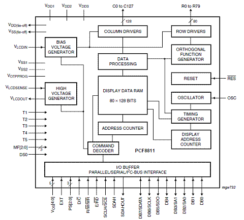
图1。PCF8811方框图

图2。PCF8811应用框图:内部电荷泵和单电源

图3。PCF8811应用框图:内部电荷泵和两个分立电源(VDD1和VDD2)
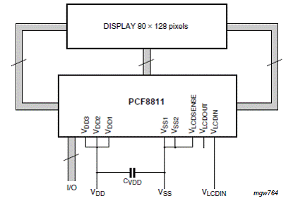
图4.PCF8811应用框图:外接高压
版权与免责声明
凡本网注明“出处:维库电子市场网”的所有作品,版权均属于维库电子市场网,转载请必须注明维库电子市场网,https://www.dzsc.com,违反者本网将追究相关法律责任。
本网转载并注明自其它出处的作品,目的在于传递更多信息,并不代表本网赞同其观点或证实其内容的真实性,不承担此类作品侵权行为的直接责任及连带责任。其他媒体、网站或个人从本网转载时,必须保留本网注明的作品出处,并自负版权等法律责任。
如涉及作品内容、版权等问题,请在作品发表之日起一周内与本网联系,否则视为放弃相关权利。
- tn-s系统是什么意思_tn-s接地系统_tn-s接地系统做法2024/6/7 17:38:31
- 什么是智能安全帽 如何选购智能安全帽?2024/6/7 17:34:26
- 卡诺图化简法例题详解2024/6/4 17:43:36
- 什么是数据库,除了MySQL还有哪些数据库?2024/6/4 17:39:36
- 如何使用secure CRT连接交换机2024/6/3 17:41:56