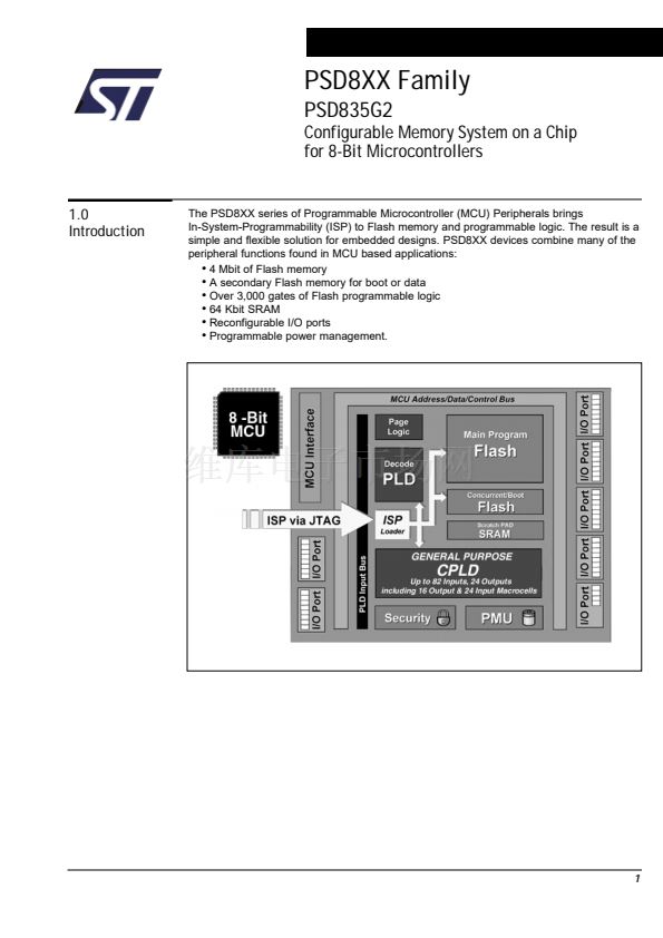
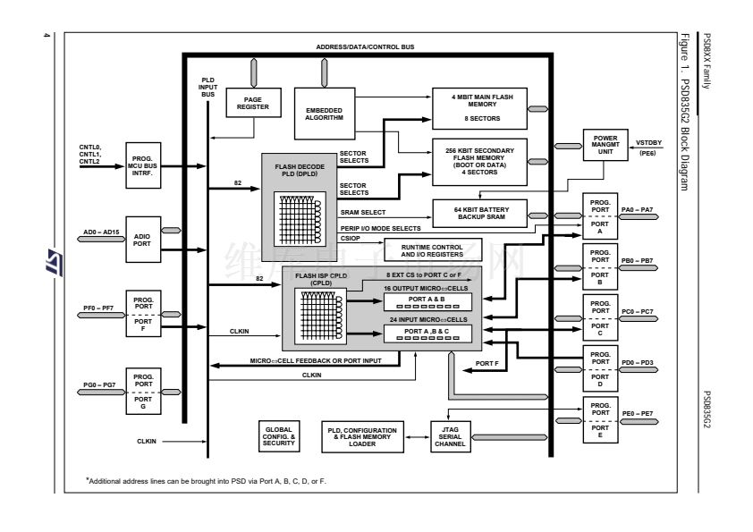
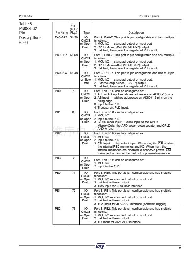
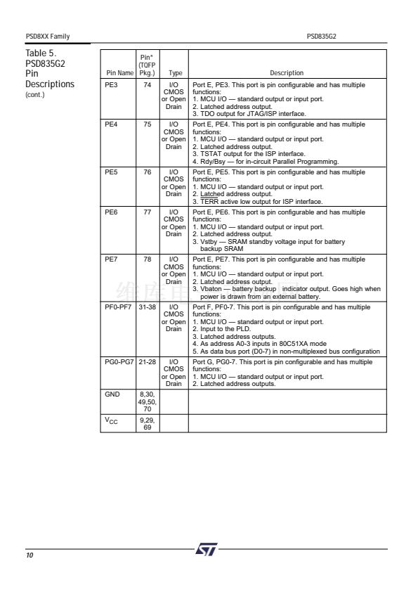
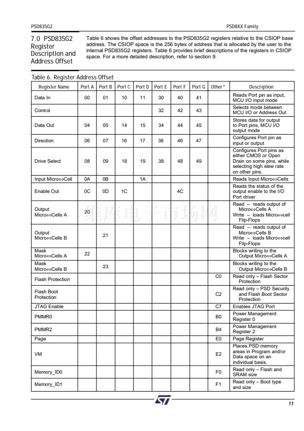
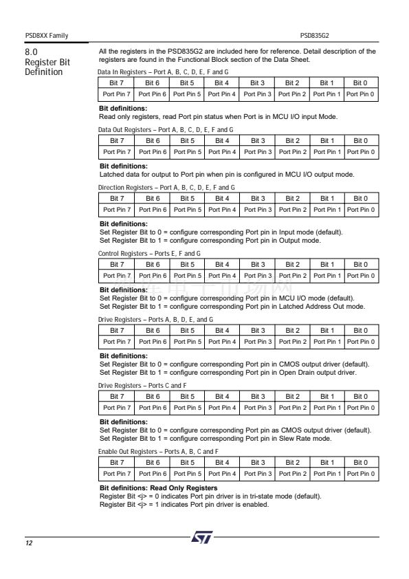
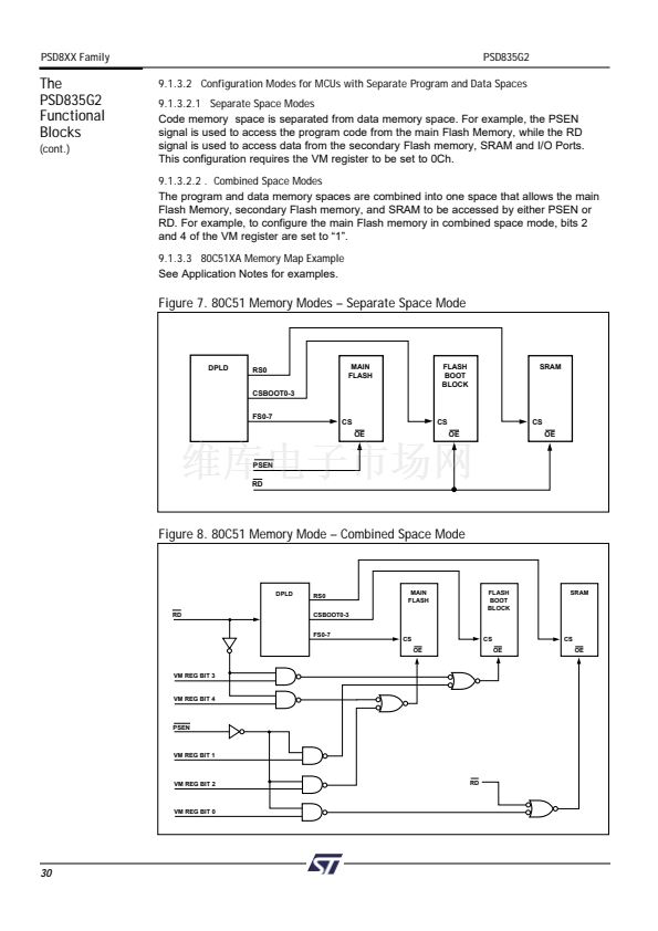
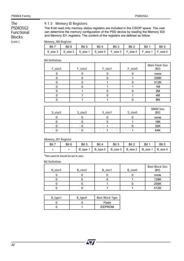
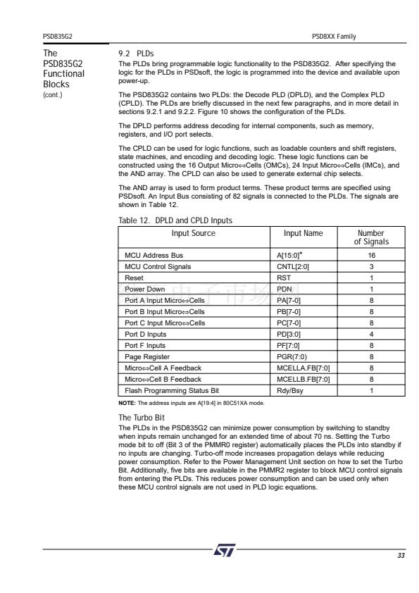
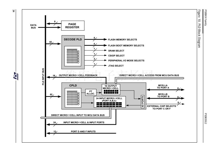
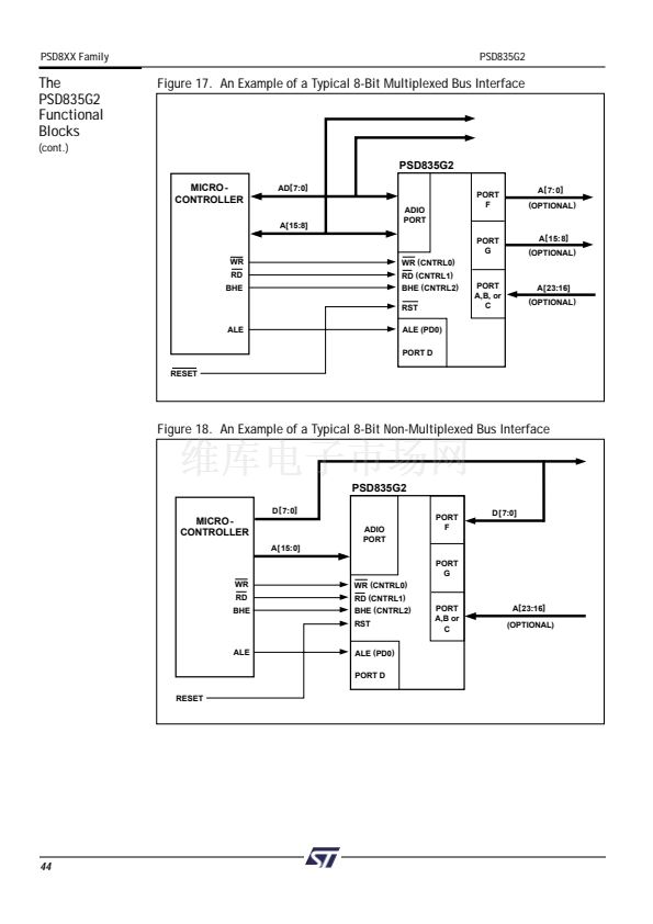
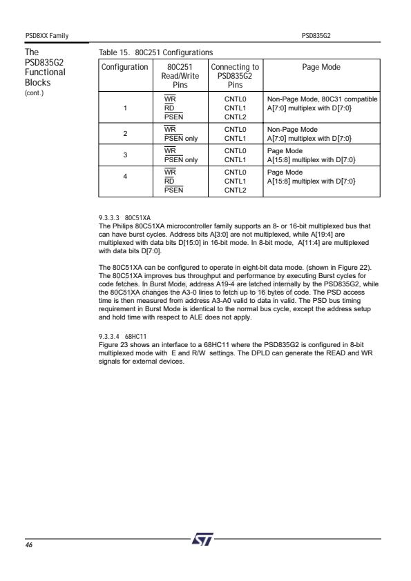
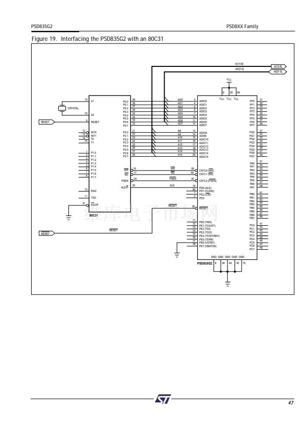
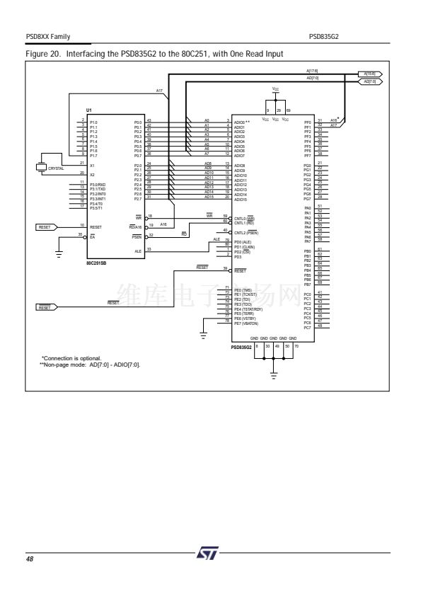
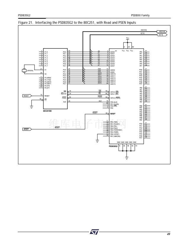
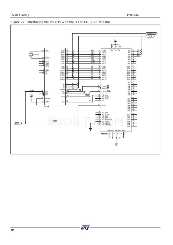
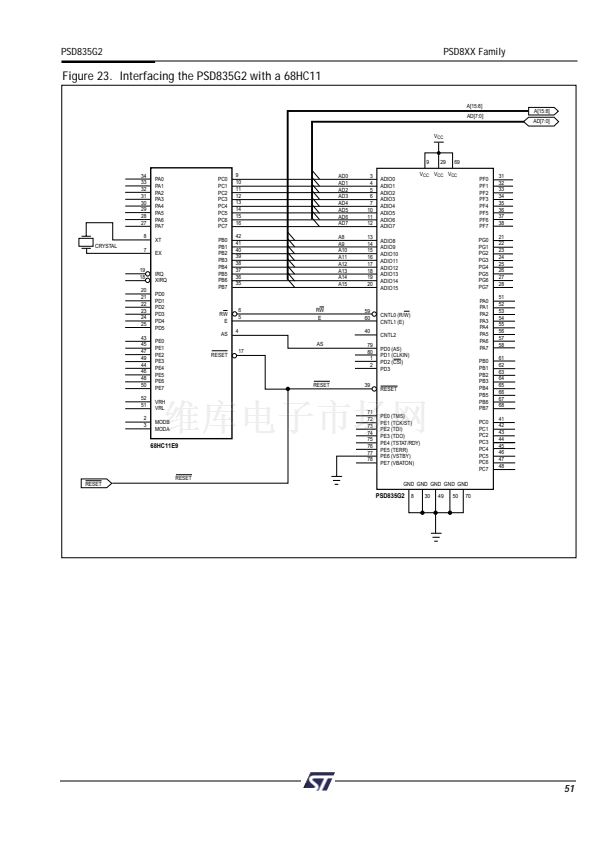
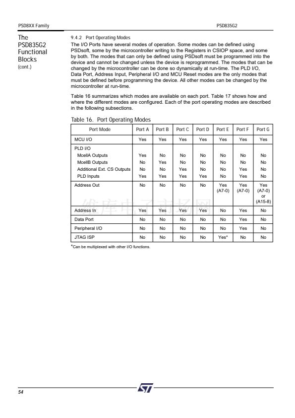
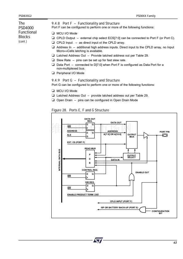
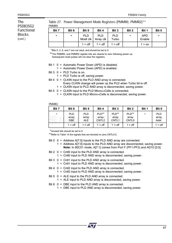
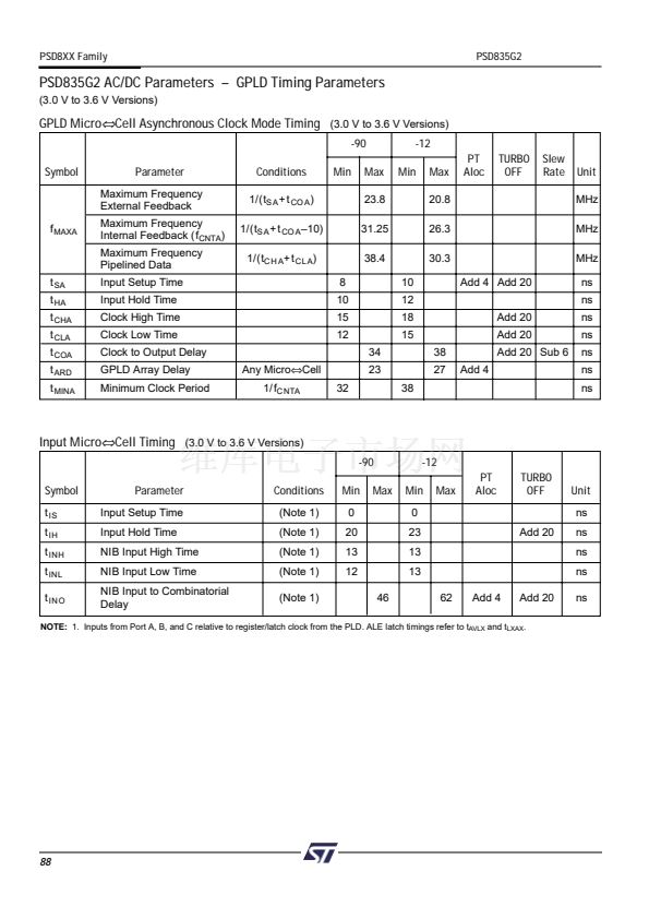
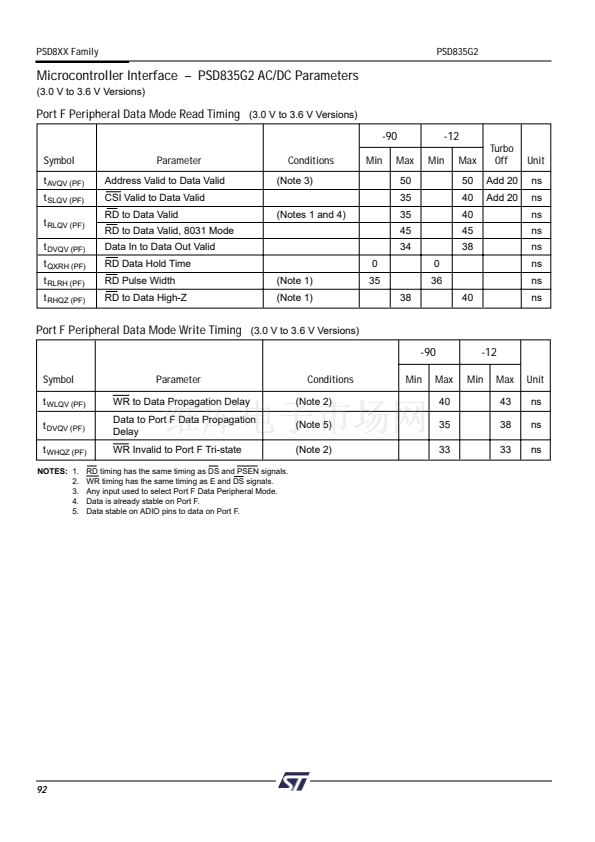
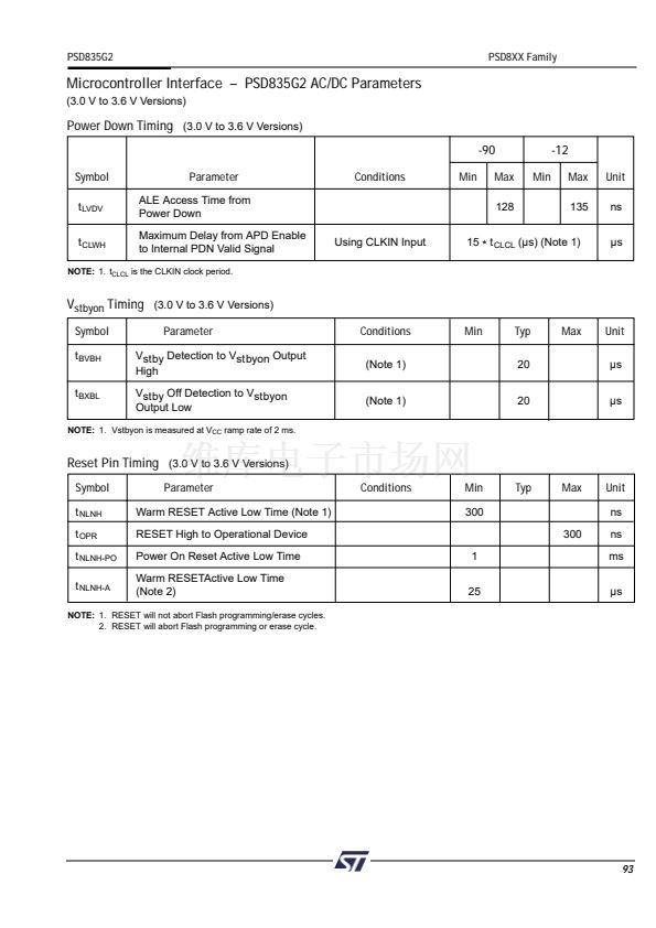
PSD8XX Family
PSD835G2
(3.0 V to 3.6 V Versions)
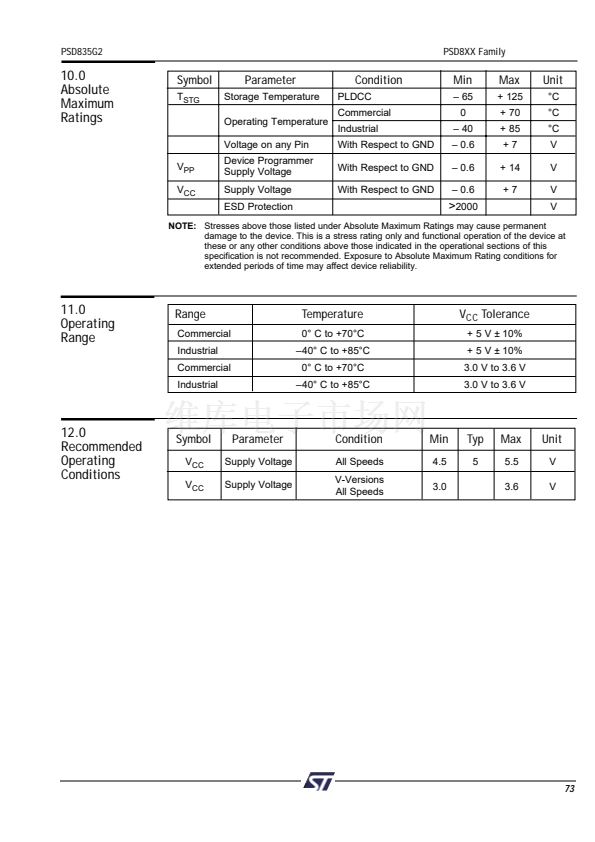
PSD835G2 DC Characteristics
Symbol
V
CC
V
IH
V
IL
V
IH1
V
IL1
V
HYS
V
LKO
V
OL
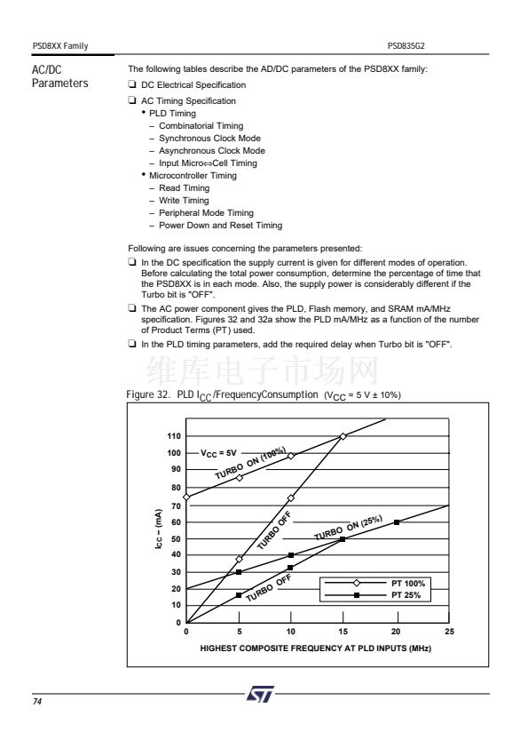
Advance Information
Min
3.0
.7 V
CC
鈥?5
.8 V
CC
鈥?5
0.3
1.5
2.3
0.01
0.15
2.9
2.7
V
SBY
鈥?0.8
2.0
V
CC
0.5
鈥?.1
2
50
鈥?
鈥?0
卤.1
卤5
100
1
10
1
0.1
2.99
2.8
0.1
0.45
Parameter
Supply Voltage
High Level Input Voltage
Low Level Input Voltage
Reset High Level Input Voltage
Reset Low Level Input Voltage
Reset Pin Hysteresis
V
CC
Min for Flash Erase and Program
Output Low Voltage
Conditions
All Speeds
3.0 V < V
CC
< 3.6 V
3.0 V < V
CC
< 3.6 V
(Note 1)
(Note 1)
Typ
Max
3.6
V
CC
+.5
0.8
V
CC
+.5
.2 V
CC
鈥?1
Unit
V
V
V
V
V
V
V
V
V
V
V
V
V
碌A
碌A
V
碌A
碌A
碌A
I
OL
= 20 碌A, V
CC
= 3.0 V
I
OL
= 4 mA, V
CC
= 3.0 V
V
OH
V
OH1
V
SBY
I
SBY
I
IDLE
V
DF
I
SB
I
LI
I
LO
I
O
Output High Voltage Except V
STBY
On
Output High Voltage V
STBY
On
SRAM Standby Voltage
SRAM Standby Current (V
STBY
Pin)
Idle Current (V
STBY
Pin)
SRAM Data Retention Voltage
Standby Supply Current
for Power Down Mode
Input Leakage Current
Output Leakage Current
Output Current
I
OH
= 鈥?0 碌A, V
CC
= 3.0 V
I
OH
= 鈥? mA, V
CC
= 3.0 V
I
OH1
= 1 碌A
V
CC
= 0 V
V
CC
> V
SBY
Only on V
STBY
CSI >V
CC
鈥?.3 V
(Notes 2 and 3)
V
SS
< V
IN
< V
CC
0.45 < V
IN
< V
CC
Refer to I
OL
and I
OH
in
the V
OL
and V
OH
row
ZPLD_TURBO = OFF,
f = 0 MHz (Note 3)
0
200
10
0
0
(Note 4)
1.5
0.8
2.0
1.5
400
25
0
0
mA
碌A/PT
mA
mA
mA
Figure 32a
mA/MHz
mA/MHz
PLD Only
I
CC
(DC)
(Note 5)
Operating
Supply Current
FLASH
ZPLD_TURBO = ON,
f = 0 MHz
During FLASH
Write/Erase Only
Read Only, f = 0 MHz
SRAM
PLD AC Base
I
CC
(AC)
(Note 5)
FLASH
AC Adder
SRAM AC Adder
NOTES:
1.
2.
3.
4.
5.
f = 0 MHz
Reset input has hysteresis. V
IL1
is valid at or below .2V
CC
鈥?1. V
IH1
is valid at or above .8V
CC
.
CSI deselected or internal PD mode is active.
PLD is in non-turbo mode and none of the inputs are switching.
Refer to Figure 31a for PLD current calculation.
I
O
= 0 mA.
86


 1
1
 2
2
 3
3
 4
4
 5
5
 6
6
 7
7
 8
8
 9
9
 10
10
 11
11
 12
12
 13
13
 14
14
 15
15
 16
16
 17
17
 18
18
 19
19
 20
20
 21
21
 22
22
 23
23
 24
24
 25
25
 26
26
 27
27
 28
28
 29
29
 30
30
 31
31
 32
32
 33
33
 34
34
 35
35
 36
36
 37
37
 38
38
 39
39
 40
40
 41
41
 42
42
 43
43
 44
44
 45
45
 46
46
 47
47
 48
48
 49
49
 50
50
 51
51
 52
52
 53
53
 54
54
 55
55
 56
56
 57
57
 58
58
 59
59
 60
60
 61
61
 62
62
 63
63
 64
64
 65
65
 66
66
 67
67
 68
68
 69
69
 70
70
 71
71
 72
72
 73
73
 74
74
 75
75
 76
76
 77
77
 78
78
 79
79
 80
80
 81
81
 82
82
 83
83
 84
84
 85
85
 86
86
 87
87
 88
88
 89
89
 90
90
 91
91
 92
92
 93
93
 94
94
 95
95
 96
96
 97
97
 98
98
 99
99
 100
100
 101
101
 102
102
 103
103
 104
104
 105
105
 106
106
 107
107
 108
108
 109
109
 110
110
