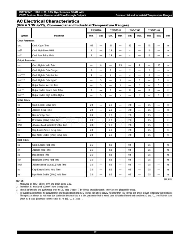
IDT71V547, 128K x 36, 3.3V Synchronous SRAM with
ZBT鈩?Feature, Burst Counter and Flow-Through Outputs
鈩?/div>
Commercial and Industrial Temperature Ranges
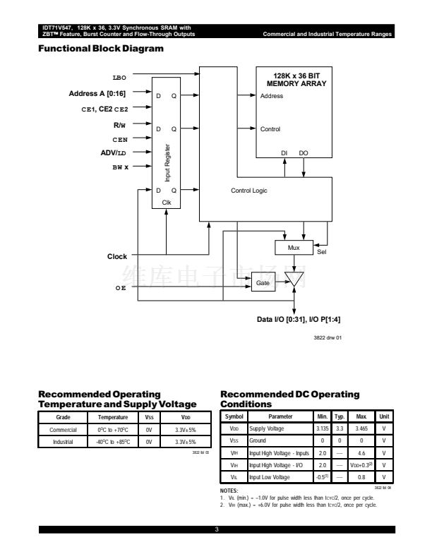
Functional Block Diagram
LBO
Address A [0:16]
C E
1
, CE2
C E
2
R/W
C EN
ADV/LD
BW
x
D
Clk
D
Q
Control
D
Q
128K x 36 BIT
MEMORY ARRAY
Address
Input Register
DI
DO
Q
Control Logic
Mux
Clock
Sel
OE
Gate
,
Data I/O [0:31], I/O P[1:4]
3822 drw 01
Recommended Operating
Temperature and Supply Voltage
Grade
Commercial
Industrial
Temperature
0
O
C to +70
O
C
-40
O
C to +85
O
C
V
SS
0V
0V
V
DD
3.3V卤5%
3.3V卤5%
3822 tbl 03
Recommended DC Operating
Conditions
Symbol
V
DD
V
SS
V
IH
V
IH
V
IL
Parameter
Supply Voltage
Ground
Input High Voltage - Inputs
Input High Voltage - I/O
Input Low Voltage
Min.
3.135
0
2.0
2.0
-0.5
(1)
Typ.
3.3
0
____
____
____
Max.
3.465
0
4.6
V
DD
+0.3
(2)
0.8
Unit
V
V
V
V
V
3822 tbl 04
NOTES:
1. V
IL
(min.) = 鈥?.0V for pulse width less than t
CYC
/2, once per cycle.
2. V
IH
(max.) = +6.0V for pulse width less than t
CYC
/2, once per cycle.
3
6.42


 1
1
 2
2
 3
3
 4
4
 5
5
 6
6
 7
7
 8
8
 9
9
 10
10
 11
11
 12
12
 13
13
 14
14
 15
15
 16
16
 17
17
 18
18
 19
19
