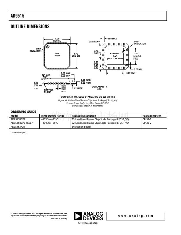
AD9515
When the delay block is OFF (bypassed), it is also powered
down.
POWER SUPPLY
The AD9515 requires a 3.3 V 卤 5% power supply for V
S
. The
tables in the Specifications section give the performance
expected from the AD9515 with the power supply voltage
within this range. In no case should the absolute maximum
range of 鈭?.3 V to +3.6 V, with respect to GND, be exceeded
on Pin VS.
Good engineering practice should be followed in the layout of
power supply traces and the ground plane of the PCB. The
power supply should be bypassed on the PCB with adequate
capacitance (>10 渭F). The AD9515 should be bypassed with
adequate capacitors (0.1 渭F) at all power pins as close as
possible to the part. The layout of the AD9515 evaluation
board (AD9515/PCB) is a good example.
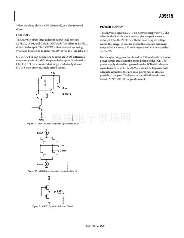
OUTPUTS
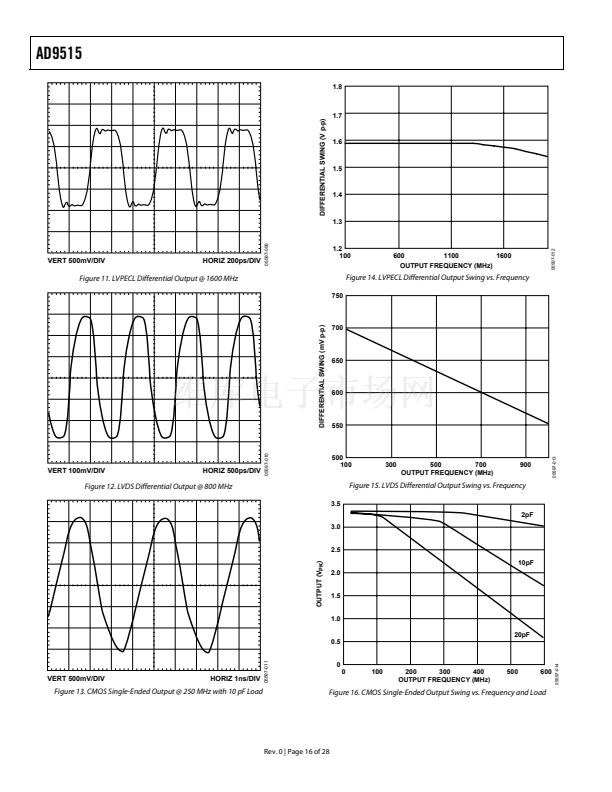
The AD9515 offers three different output level choices:
LVPECL, LVDS, and CMOS. OUT0/OUT0B offers an LVPECL
differential output. The LVPECL differential voltage swing
(V
OD
) can be selected as either 400 mV or 790 mV (see Table 11).
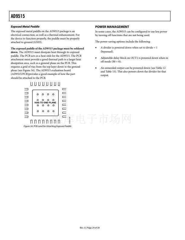
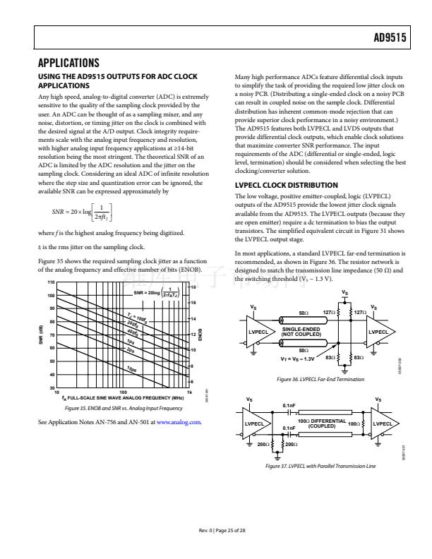
OUT1/OUT1B can be selected as either an LVDS differential
output or a pair of CMOS single-ended outputs. If selected as
CMOS, OUT1 is a noninverted, single-ended output, and
OUT1B is an inverted, single-ended output.
3.3V
OUT
OUTB
GND
Figure 31. LVPECL Output Simplified Equivalent Circuit
3.5mA
OUT
OUTB
3.5mA
Figure 32. LVDS Output Simplified Equivalent Circuit
V
S
OUT1/
OUT1B
05597-028
Figure 33. CMOS Equivalent Output Circuit
05597-027
05597-026
Rev. 0 | Page 23 of 28


 1
1
 2
2
 3
3
 4
4
 5
5
 6
6
 7
7
 8
8
 9
9
 10
10
 11
11
 12
12
 13
13
 14
14
 15
15
 16
16
 17
17
 18
18
 19
19
 20
20
 21
21
 22
22
 23
23
 24
24
 25
25
 26
26
 27
27
 28
28
