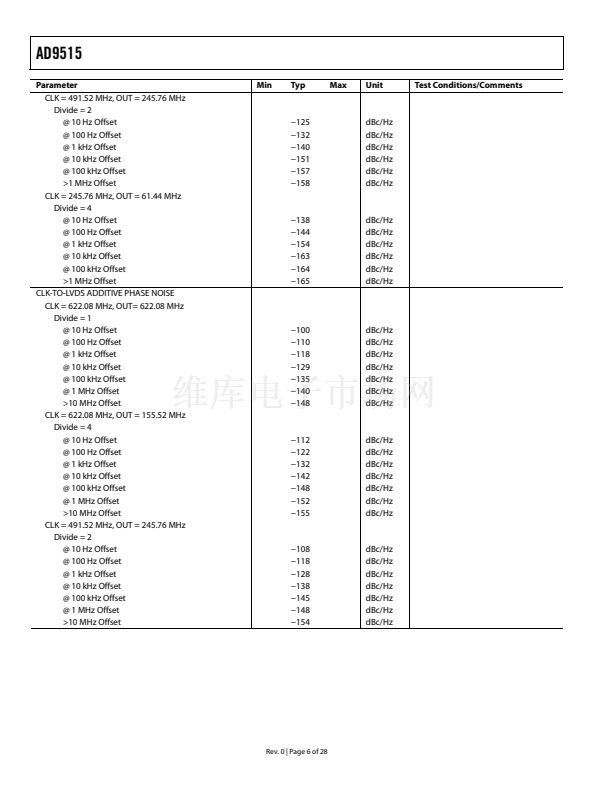
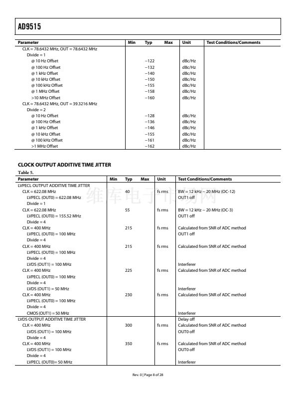
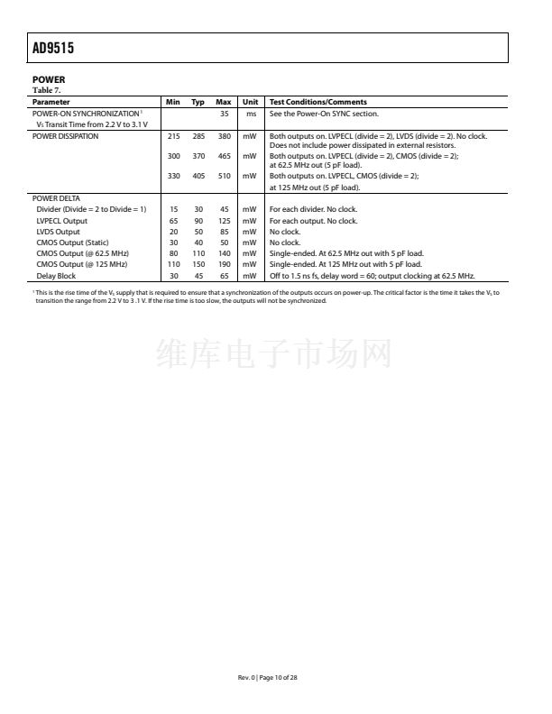
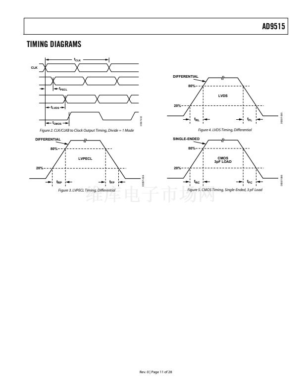
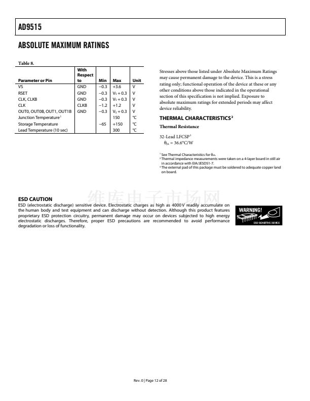
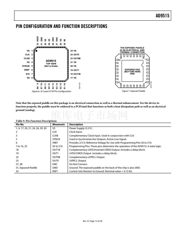
AD9515
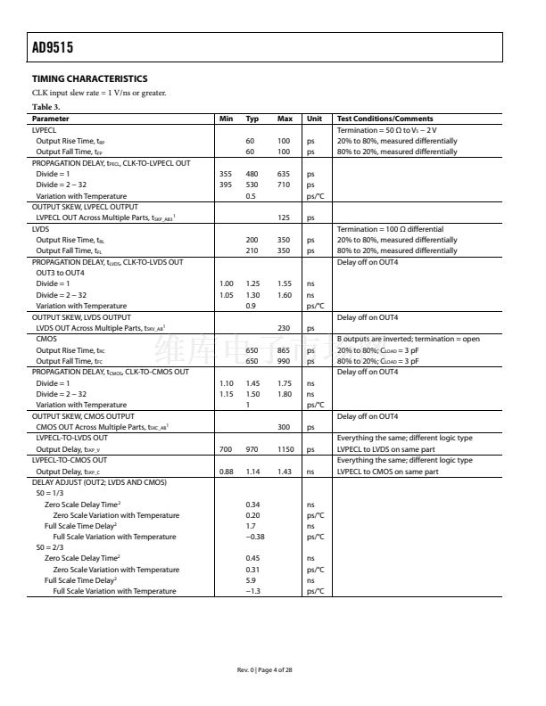
TIMING CHARACTERISTICS
CLK input slew rate = 1 V/ns or greater.
Table 3.
Parameter
LVPECL
Output Rise Time, t
RP
Output Fall Time, t
FP
PROPAGATION DELAY, t
PECL
, CLK-TO-LVPECL OUT
Divide = 1
Divide = 2 鈭?32
Variation with Temperature
OUTPUT SKEW, LVPECL OUTPUT
LVPECL OUT Across Multiple Parts, t
SKP_AB3 1
LVDS
Output Rise Time, t
RL
Output Fall Time, t
FL
PROPAGATION DELAY, t
LVDS
, CLK-TO-LVDS OUT
OUT3 to OUT4
Divide = 1
Divide = 2 鈭?32
Variation with Temperature
OUTPUT SKEW, LVDS OUTPUT
LVDS OUT Across Multiple Parts, t
SKV_AB1
CMOS
Output Rise Time, t
RC
Output Fall Time, t
FC
PROPAGATION DELAY, t
CMOS
, CLK-TO-CMOS OUT
Divide = 1
Divide = 2 鈭?32
Variation with Temperature
OUTPUT SKEW, CMOS OUTPUT
CMOS OUT Across Multiple Parts, t
SKC_AB1
LVPECL-TO-LVDS OUT
Output Delay, t
SKP_V
LVPECL-TO-CMOS OUT
Output Delay, t
SKP_C
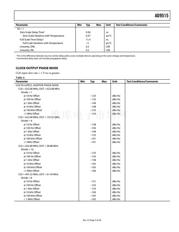
DELAY ADJUST (OUT2; LVDS AND CMOS)
S0 = 1/3
Zero Scale Delay Time
2
Zero Scale Variation with Temperature
Full Scale Time Delay
2
Full Scale Variation with Temperature
S0 = 2/3
Zero Scale Delay Time
2
Zero Scale Variation with Temperature
Full Scale Time Delay
2
Full Scale Variation with Temperature
Min
Typ
60
60
355
395
480
530
0.5
Max
100
100
635
710
Unit
ps
ps
ps
ps
ps/掳C
ps
ps
ps
Termination = 100 惟 differential
20% to 80%, measured differentially
80% to 20%, measured differentially
Delay off on OUT4
Test Conditions/Comments
Termination = 50 惟 to V
S
鈭?2 V
20% to 80%, measured differentially
80% to 20%, measured differentially
125
200
210
350
350
1.00
1.05
1.25
1.30
0.9
1.55
1.60
ns
ns
ps/掳C
Delay off on OUT4
ps
ps
ps
ns
ns
ps/掳C
Delay off on OUT4
ps
ps
ns
Everything the same; different logic type
LVPECL to LVDS on same part
Everything the same; different logic type
LVPECL to CMOS on same part
B outputs are inverted; termination = open
20% to 80%; C
LOAD
= 3 pF
80% to 20%; C
LOAD
= 3 pF
Delay off on OUT4
230
650
650
1.10
1.15
1.45
1.50
1
865
990
1.75
1.80
300
700
0.88
970
1.14
1150
1.43
0.34
0.20
1.7
鈭?.38
0.45
0.31
5.9
鈭?.3
ns
ps/掳C
ns
ps/掳C
ns
ps/掳C
ns
ps/掳C
Rev. 0 | Page 4 of 28


 1
1
 2
2
 3
3
 4
4
 5
5
 6
6
 7
7
 8
8
 9
9
 10
10
 11
11
 12
12
 13
13
 14
14
 15
15
 16
16
 17
17
 18
18
 19
19
 20
20
 21
21
 22
22
 23
23
 24
24
 25
25
 26
26
 27
27
 28
28
