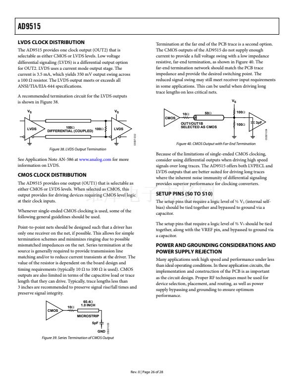
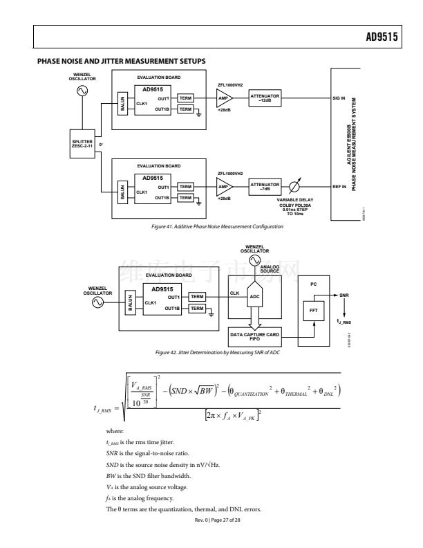
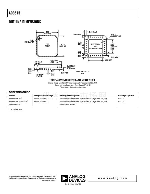
鈥?/div>
that are not turned OFF
where the divider is not divide = 1 (divider bypassed)
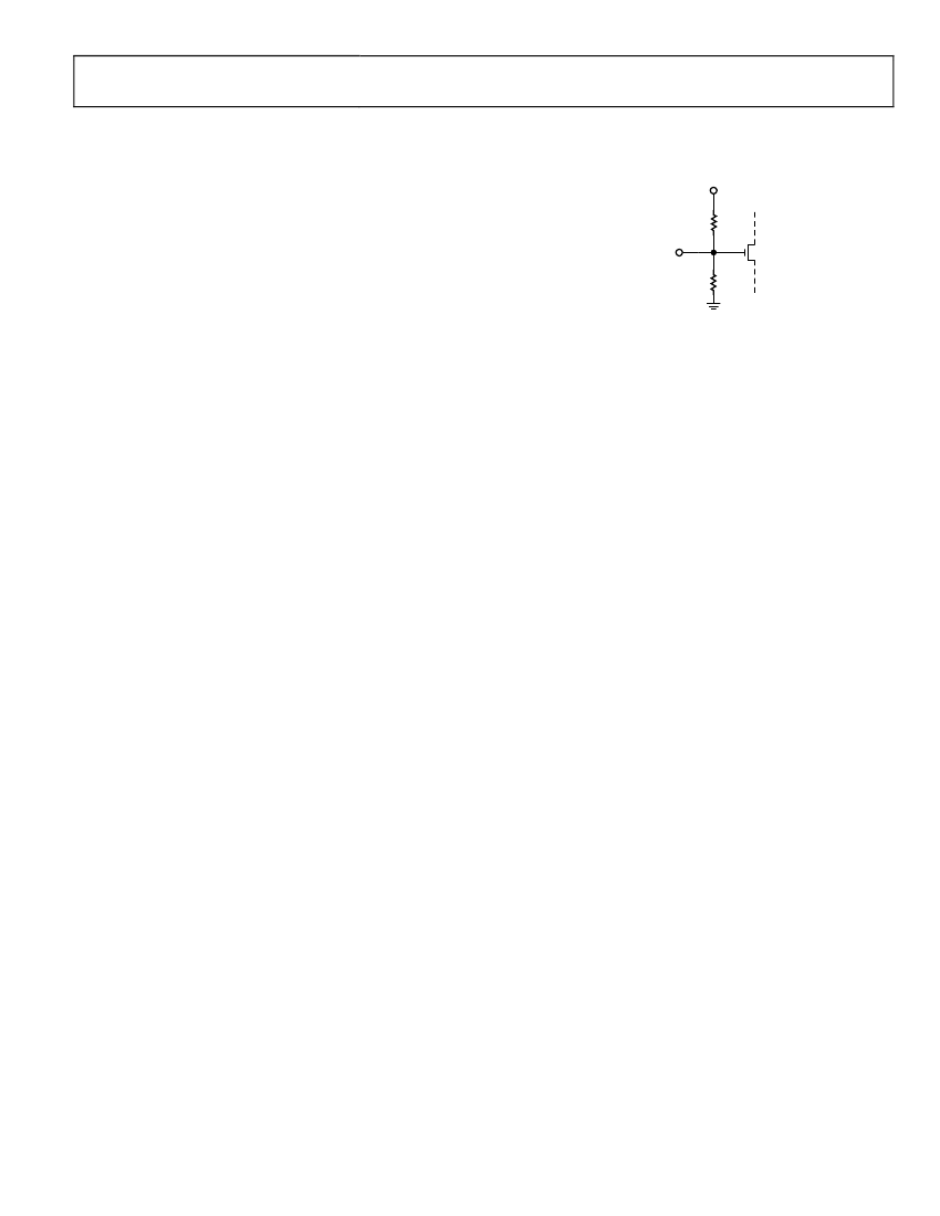
SETUP PIN
S0 TO S10
05597-023
provided by the VREF pin. All setup pins requiring the 鈪擵
S
level must be tied to the VREF pin.
V
S
60k惟
30k惟
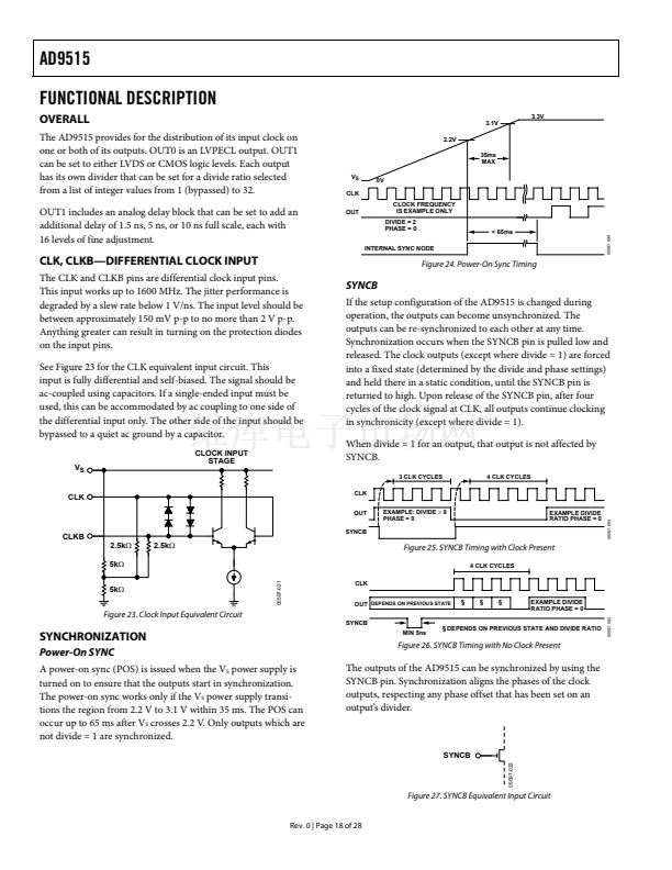
An output with its divider set to divide = 1 (divider bypassed)
is always synchronized with the input clock, with a propagation
delay.
The SYNCB pin must be pulled up for normal operation. Do
not let the SYNCB pin float.
Figure 28. Setup Pin (S0 to S10) Equivalent Circuit
R
SET
RESISTOR
The internal bias currents of the AD9515 are set by the
R
SET
resistor. This resistor should be as close as possible to
the value given as a condition in the Specifications section
(R
SET
= 4.12 k惟). This is a standard 1% resistor value and should
be readily obtainable. The bias currents set by this resistor
determine the logic levels and operating conditions of the
internal blocks of the AD9515. The performance figures given
in the Specifications section assume that this resistor value is
used for R
SET
.
The AD9515 operation is determined by the combination of
logic levels present at the setup pins. The setup configurations
for the AD9515 are shown in Table 10 to Table 15. The four
logic levels are referred to as 0, 鈪? 鈪? and 1. These numbers
represent the fraction of the V
S
voltage that defines the logic
levels. See the setup pin thresholds in Table 6.
The meaning of some of the setup pins depends on the logic
level set on other pins. For example, the effect of the S9/S10 pair
of pins depends on the state of S8. S8 selects whether the phase
value selected by S9/S10 affects either OUT0 or OUT1. In
addition, if OUT1 is selected to have its phase controlled, the
effect further depends on the state of S0. If S = 0, the delay block
for OUT1 is bypassed, and the logic levels on S9/S10 set the
phase value of the OUT1 divider. However, if S0 鈮?0, then the
full-scale delay for OUT1 is set by the logic level on S0, and
S9/S10 set the delay block fine delay (fraction of full scale).
Additionally, if a nonzero phase value is selected by S2/S3/S4
(for OUT0) or S5/S6/S7 (for OUT1), this phase overrides the
phase value selected by S9/S10. This allows a phase delay to be
selected on OUT0 while also selecting a time delay on OUT1.
S1 selects the logic level of each output. OUT0 is LVPECL. The
LVPECL output differential voltage (V
OD
) can be selected from
two levels: 400 mV or 780 mV. OUT1 can be set to either LVDS
or CMOS levels.
OUT0 can be turned off (powered down) by setting S2/S3/S4 to
0/1/0. OUT1 can be turned off by setting S5/S6/S7 to 0/1/0.
Do not set S2/S3/S4/S5/S6/S7 to 1/1/1/1/1/1.
VREF
The VREF pin provides a voltage level of 鈪?V
S
. This voltage is
one of the four logic levels used by the setup pins (S0 to S10).
These pins set the operation of the AD9515. The VREF pin
provides sufficient drive capability to drive as many of the setup
pins as necessary, up to all on a single part. The VREF pin
should be used for no other purpose.
SETUP CONFIGURATION
The specific operation of the AD9515 is set by the logic levels
applied to the setup pins (S10 to S0). These pins use four-state
logic. The logic levels used are V
S
and GND, plus 鈪?V
S
and
鈪?V
S
. The 鈪?V
S
level is provided by the internal self-biasing on
each of the setup pins (S10 to S0). This is the level seen by a
setup pin that is left not connected (NC). The 鈪?V
S
level is
Rev. 0 | Page 19 of 28


 1
1
 2
2
 3
3
 4
4
 5
5
 6
6
 7
7
 8
8
 9
9
 10
10
 11
11
 12
12
 13
13
 14
14
 15
15
 16
16
 17
17
 18
18
 19
19
 20
20
 21
21
 22
22
 23
23
 24
24
 25
25
 26
26
 27
27
 28
28
