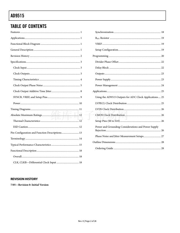
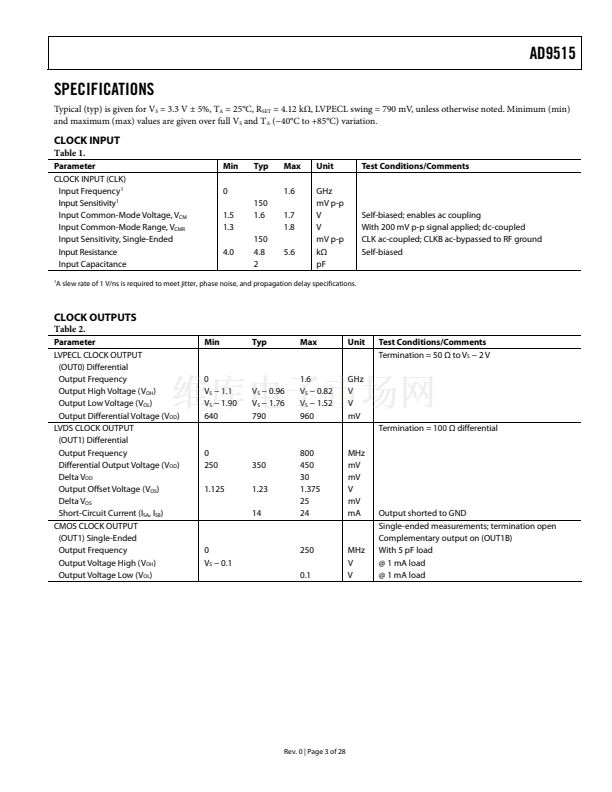
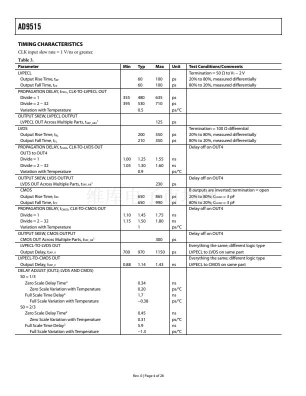
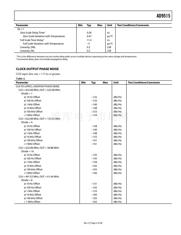
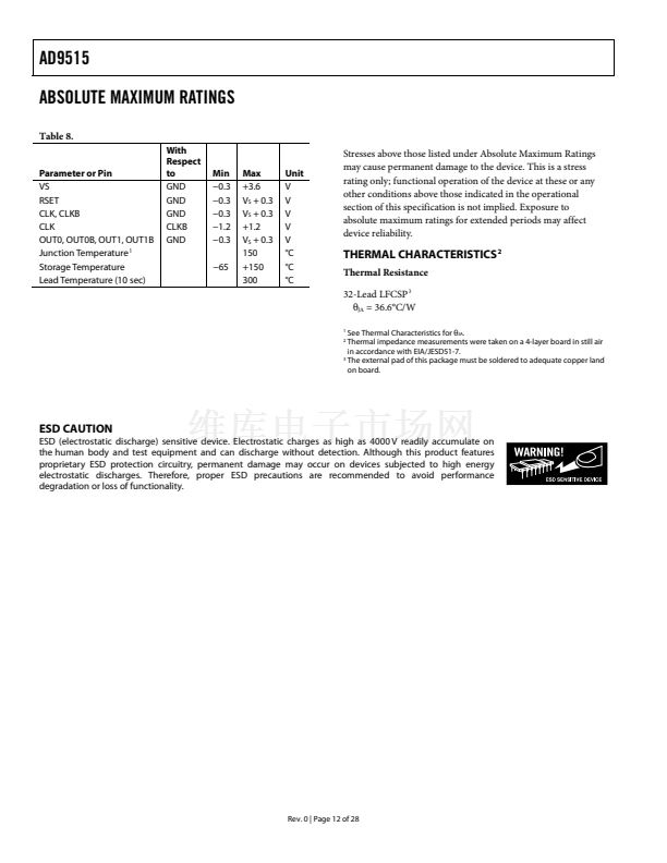
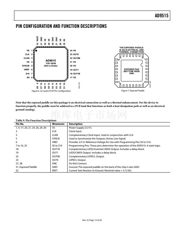
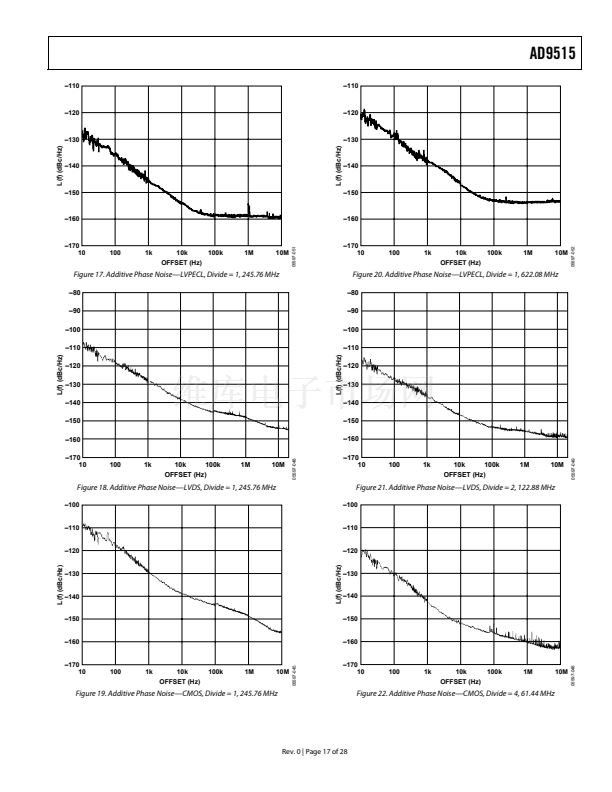
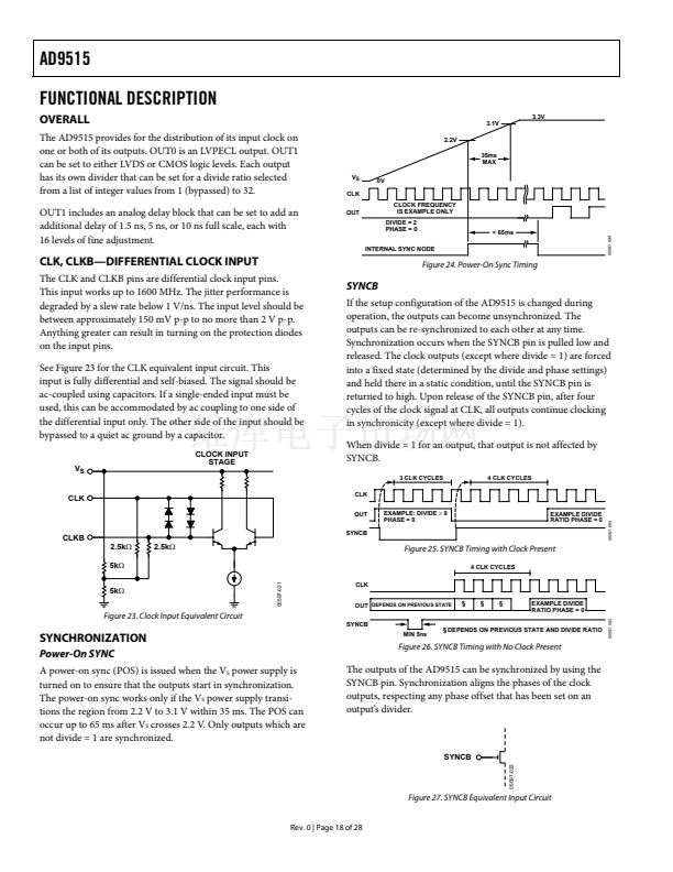
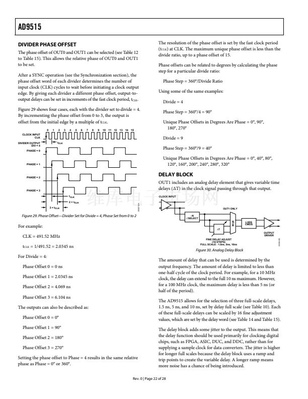
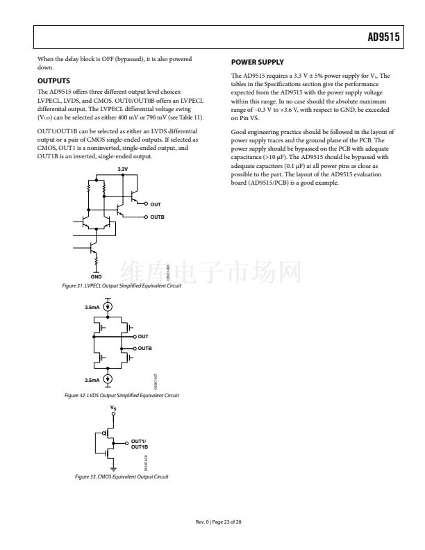
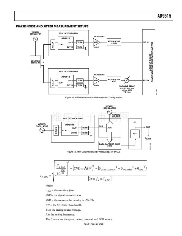
AD9515
LVDS CLOCK DISTRIBUTION
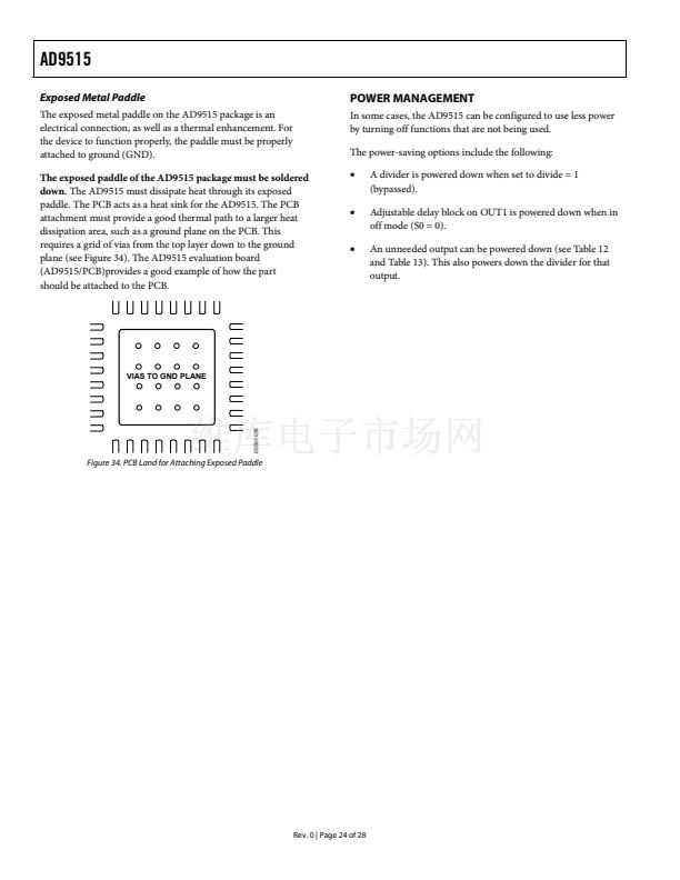
The AD9515 provides one clock output (OUT2) that is
selectable as either CMOS or LVDS levels. Low voltage
differential signaling
(
LVDS) is a differential output option
for OUT2. LVDS uses a current mode output stage. The
current is 3.5 mA, which yields 350 mV output swing across
a 100 惟 resistor. The LVDS output meets or exceeds all
ANSI/TIA/EIA-644 specifications.
A recommended termination circuit for the LVDS outputs
is shown in Figure 38.
V
S
V
S
CMOS
Termination at the far end of the PCB trace is a second option.
The CMOS outputs of the AD9515 do not supply enough
current to provide a full voltage swing with a low impedance
resistive, far-end termination, as shown in Figure 40. The
far-end termination network should match the PCB trace
impedance and provide the desired switching point. The
reduced signal swing may still meet receiver input requirements
in some applications. This can be useful when driving long
trace lengths on less critical nets.
V
S
50惟
100惟
3pF
05597-034
10惟
LVDS
100惟
100惟
DIFFERENTIAL (COUPLED)
LVDS
05597-032
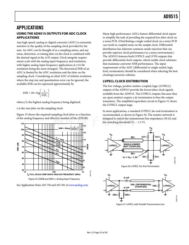
OUT1/OUT1B
SELECTED AS CMOS
100惟
Figure 40. CMOS Output with Far-End Termination
Figure 38. LVDS Output Termination
See Application Note AN-586 at
www.analog.com
for more
information on LVDS.
CMOS CLOCK DISTRIBUTION
The AD9515 provides one output (OUT1) that is selectable as
either CMOS or LVDS levels. When selected as CMOS, this
output provides for driving devices requiring CMOS level logic
at their clock inputs.
Whenever single-ended CMOS clocking is used, some of the
following general guidelines should be used.
Point-to-point nets should be designed such that a driver has
only one receiver on the net, if possible. This allows for simple
termination schemes and minimizes ringing due to possible
mismatched impedances on the net. Series termination at the
source is generally required to provide transmission line
matching and/or to reduce current transients at the driver. The
value of the resistor is dependent on the board design and
timing requirements (typically 10 惟 to 100 惟 is used). CMOS
outputs are also limited in terms of the capacitive load or trace
length that they can drive. Typically, trace lengths less than
3 inches are recommended to preserve signal rise/fall times and
preserve signal integrity.
10惟
CMOS
MICROSTRIP
05597-033
Because of the limitations of single-ended CMOS clocking,
consider using differential outputs when driving high speed
signals over long traces. The AD9515 offers both LVPECL and
LVDS outputs that are better suited for driving long traces
where the inherent noise immunity of differential signaling
provides superior performance for clocking converters.
SETUP PINS (S0 TO S10)
The setup pins that require a logic level of 鈪?V
S
(internal self-
bias) should be tied together and bypassed to ground via a
capacitor.
The setup pins that require a logic level of 鈪?V
S
should be tied
together, along with the VREF pin, and bypassed to ground via
a capacitor.
POWER AND GROUNDING CONSIDERATIONS AND
POWER SUPPLY REJECTION
Many applications seek high speed and performance under less
than ideal operating conditions. In these application circuits, the
implementation and construction of the PCB is as important
as the circuit design. Proper RF techniques must be used for
device selection, placement, and routing, as well as power
supply bypassing and grounding to ensure optimum
performance.
60.4惟
1.0 INCH
5pF
GND
Figure 39. Series Termination of CMOS Output
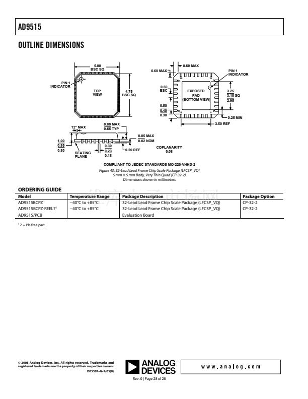
Rev. 0 | Page 26 of 28


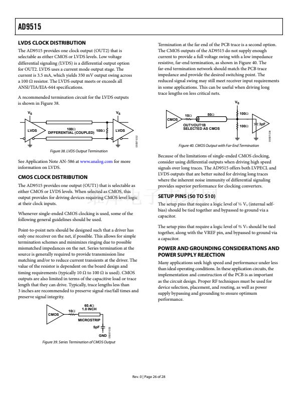
 1
1
 2
2
 3
3
 4
4
 5
5
 6
6
 7
7
 8
8
 9
9
 10
10
 11
11
 12
12
 13
13
 14
14
 15
15
 16
16
 17
17
 18
18
 19
19
 20
20
 21
21
 22
22
 23
23
 24
24
 25
25
 26
26
 27
27
 28
28
