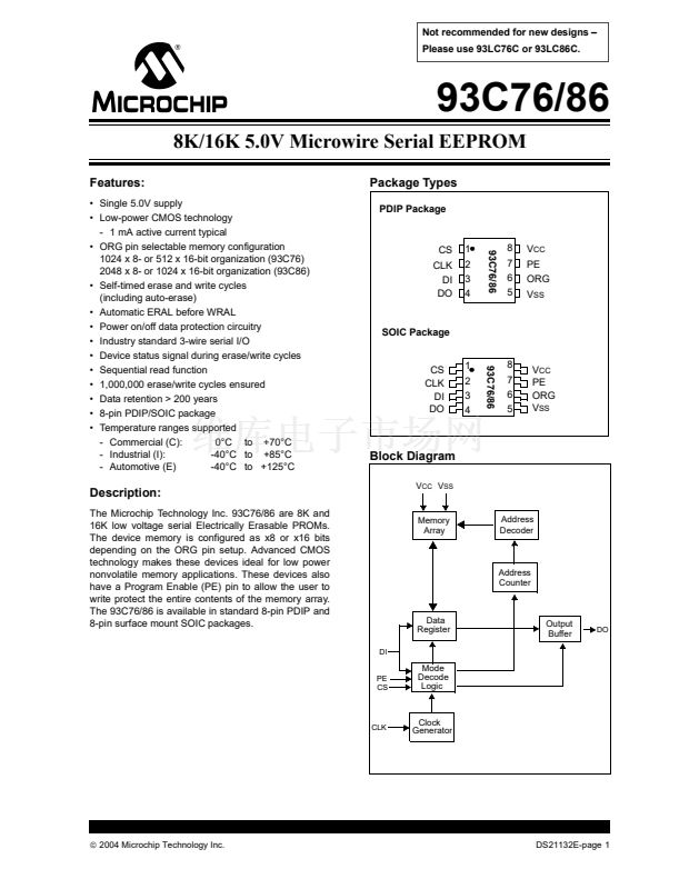
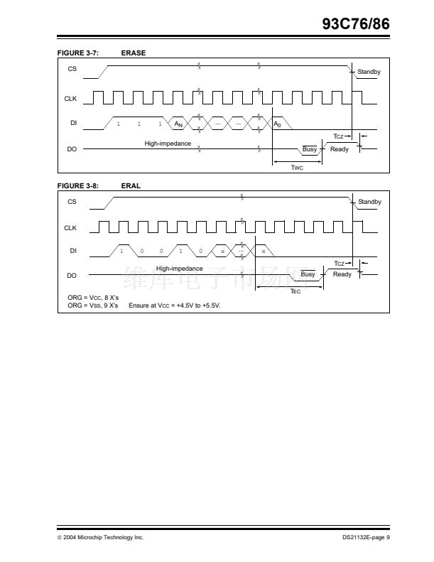
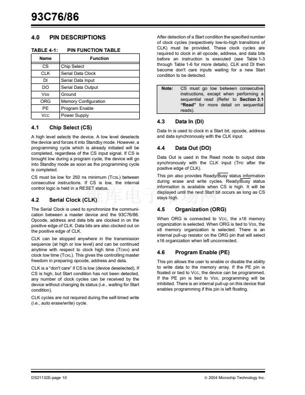
93C76/86
4.0
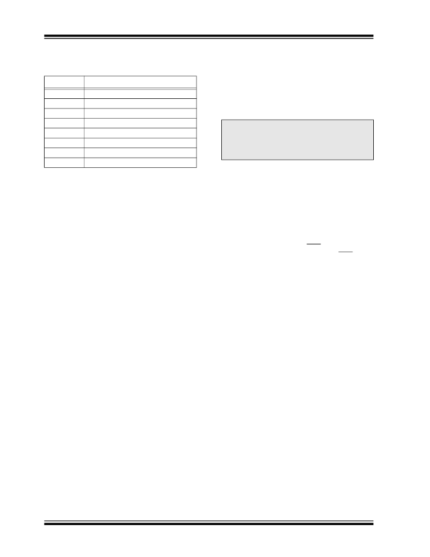
PIN DESCRIPTIONS
PIN FUNCTION TABLE
Function
Chip Select
Serial Data Clock
Serial Data Input
Serial Data Output
Ground
Memory Configuration
Program Enable
Power Supply
Note:
CS must go low between consecutive
instructions, except when performing a
sequential read (Refer to
Section 3.1
鈥淩ead鈥?/span>
for more detail on sequential
reads).
TABLE 4-1:
Name
CS
CLK
DI
DO
V
SS
ORG
PE
V
CC
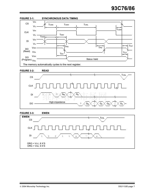
After detection of a Start condition the specified number
of clock cycles (respectively low-to-high transitions of
CLK) must be provided. These clock cycles are
required to clock in all opcode, address, and data bits
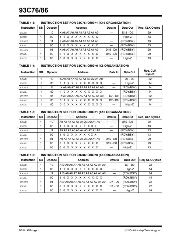
before an instruction is executed (see Table 1-3
through Table 1-6 for more details). CLK and DI then
become don't care inputs waiting for a new Start
condition to be detected.
4.3
4.1
Chip Select (CS)
A high level selects the device. A low level deselects
the device and forces it into Standby mode. However, a
programming cycle which is already initiated will be
completed, regardless of the CS input signal. If CS is
brought low during a program cycle, the device will go
into Standby mode as soon as the programming cycle
is completed.
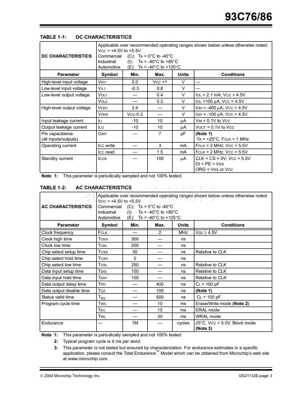
CS must be low for 250 ns minimum (T
CSL
) between
consecutive instructions. If CS is low, the internal
control logic is held in a RESET status.
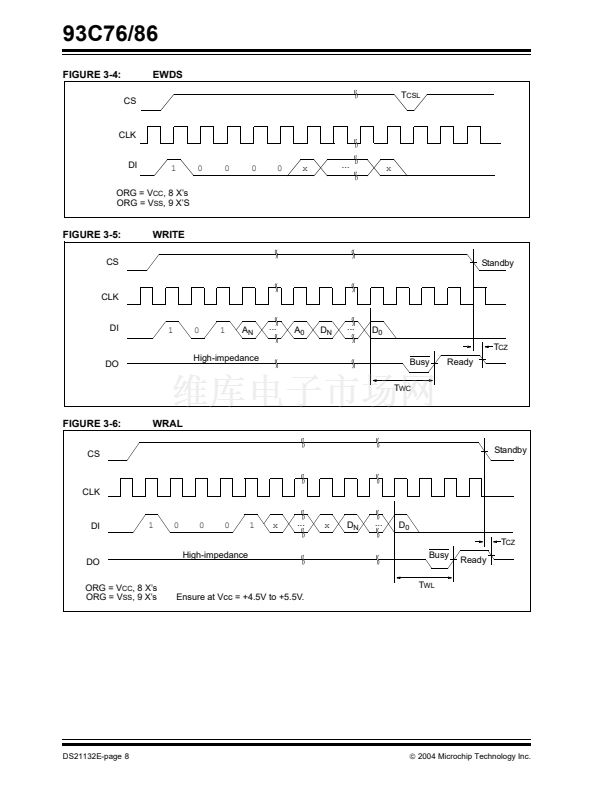
Data In (DI)
Data In is used to clock in a Start bit, opcode, address
and data synchronously with the CLK input.
4.4
Data Out (DO)
Data Out is used in the Read mode to output data
synchronously with the CLK input (T
PD
after the
positive edge of CLK).
This pin also provides Ready/Busy status information
during erase and write cycles. Ready/Busy status
information is available when CS is high. It will be
displayed until the next Start bit occurs as long as CS
stays high.
4.2
Serial Clock (CLK)
The Serial Clock is used to synchronize the communi-
cation between a master device and the 93C76/86.
Opcode, address and data bits are clocked in on the
positive edge of CLK. Data bits are also clocked out on
the positive edge of CLK.
CLK can be stopped anywhere in the transmission
sequence (at high or low level) and can be continued
anytime with respect to clock high time (T
CKH
) and
clock low time (T
CKL
). This gives the controlling master
freedom in preparing opcode, address and data.
CLK is a 鈥渄on't care鈥?if CS is low (device deselected). If
CS is high, but Start condition has not been detected,
any number of clock cycles can be received by the
device without changing its status (i.e., waiting for Start
condition).
CLK cycles are not required during the self-timed write
(i.e., auto erase/write) cycle.
4.5
Organization (ORG)
When ORG is connected to V
CC
, the x16 memory
organization is selected. When ORG is tied to V
SS
, the
x8 memory organization is selected. There is an
internal pull-up resistor on the ORG pin that will select
x16 organization when left unconnected.
4.6
Program Enable (PE)
This pin allows the user to enable or disable the ability
to write data to the memory array. If the PE pin is
floated or tied to V
CC
, the device can be programmed.
If the PE pin is tied to V
SS
, programming will be
inhibited. There is an internal pull-up on this device that
enables programming if this pin is left floating.
DS21132E-page 10
铮?/div>
2004 Microchip Technology Inc.


 1
1
 2
2
 3
3
 4
4
 5
5
 6
6
 7
7
 8
8
 9
9
 10
10
 11
11
 12
12
 13
13
 14
14
 15
15
 16
16
 17
17
 18
18
 19
19
 20
20
