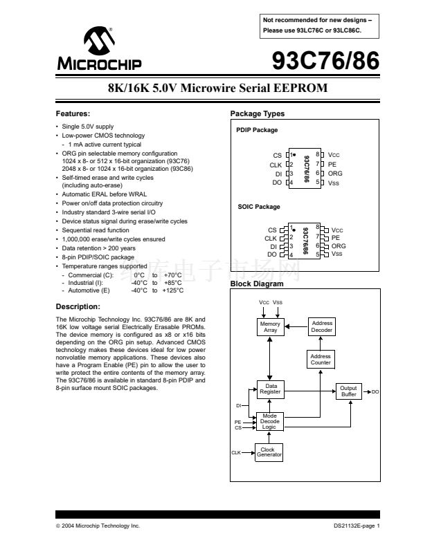
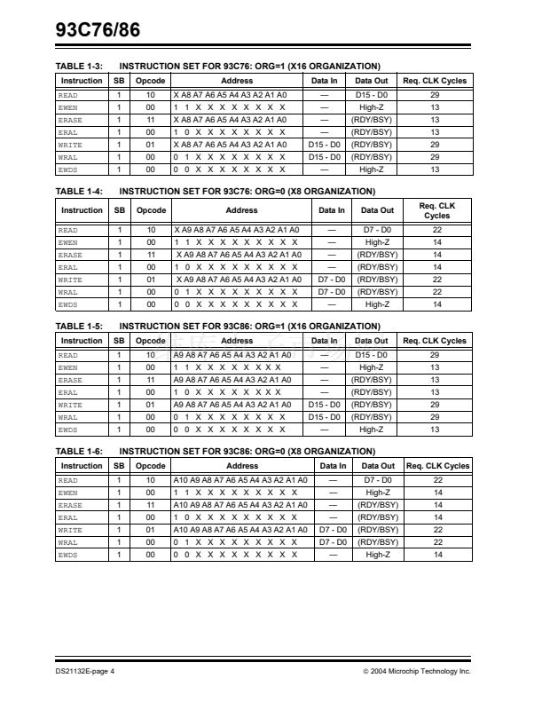
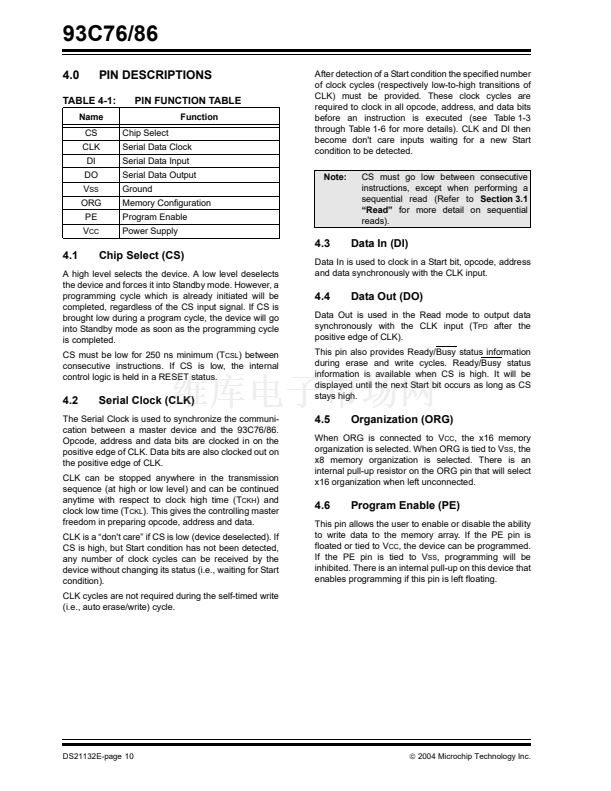
93C76/86
1.0
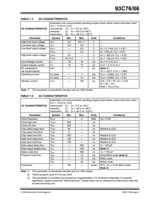
ELECTRICAL CHARACTERISTICS
Absolute Maximum Ratings
(鈥?
V
CC
.............................................................................................................................................................................7.0V
All inputs and outputs w.r.t. V
SS
........................................................................................................ -0.6V to Vcc + 1.0V
Storage temperature ...............................................................................................................................-65掳C to +150掳C
Ambient temperature with power applied ................................................................................................-40掳C to +125掳C
Soldering temperature of leads (10 seconds) .......................................................................................................+300掳C
ESD protection on all pins ..........................................................................................................................................4 kV
鈥?NOTICE: Stresses above those listed under 鈥淎bsolute Maximum Ratings鈥?may cause permanent damage to the
device. This is a stress rating only and functional operation of the device at these or any other conditions above those
indicated in the operational listings of this specification is not implied. Exposure to Absolute Maximum Rating
conditions for extended periods may affect device reliability.
1.1
AC Test Conditions
V
LO
= 2.0V
V
HI
= Vcc - 0.2V
V
HI
= 4.0V for
(Note 1)
(Note 2)
AC Waveform:
Timing Measurement Reference Level
Input
Output
Note 1:
2:
For V
CC
鈮?/div>
4.0V
For V
CC
> 4.0V
0.5 V
CC
0.5 V
CC
DS21132E-page 2
铮?/div>
2004 Microchip Technology Inc.


 1
1
 2
2
 3
3
 4
4
 5
5
 6
6
 7
7
 8
8
 9
9
 10
10
 11
11
 12
12
 13
13
 14
14
 15
15
 16
16
 17
17
 18
18
 19
19
 20
20
