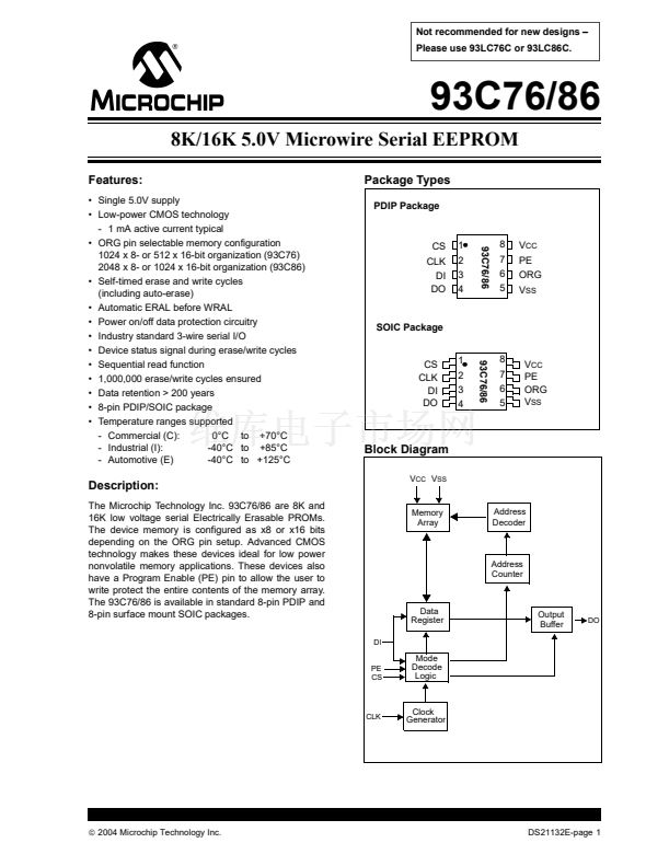
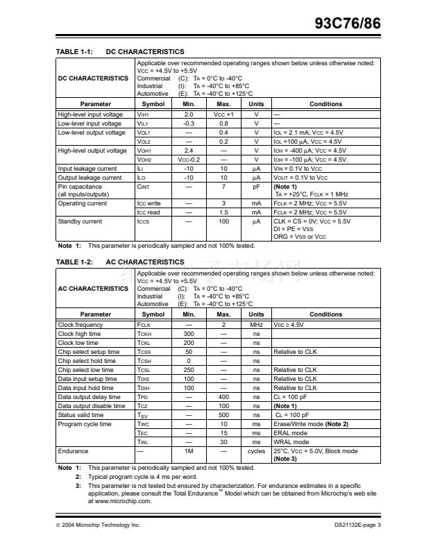
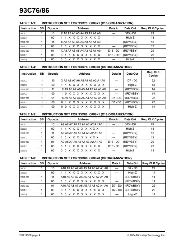
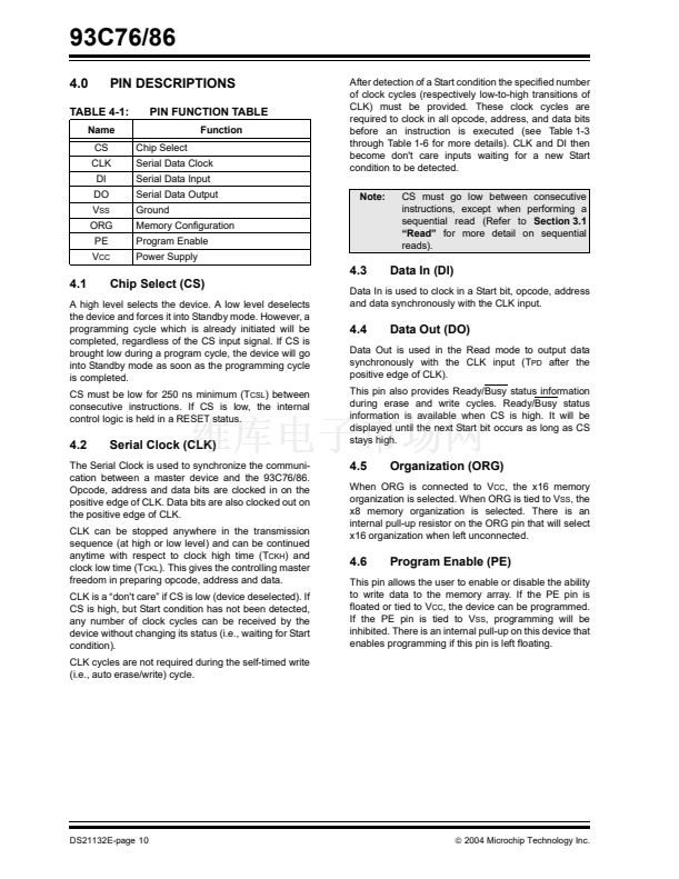
93C76/86
3.0
3.1
DEVICE OPERATION
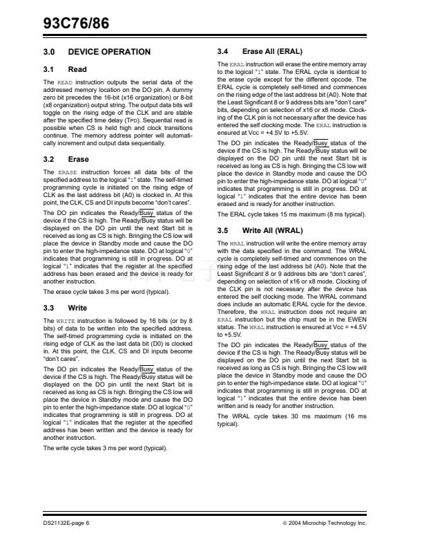
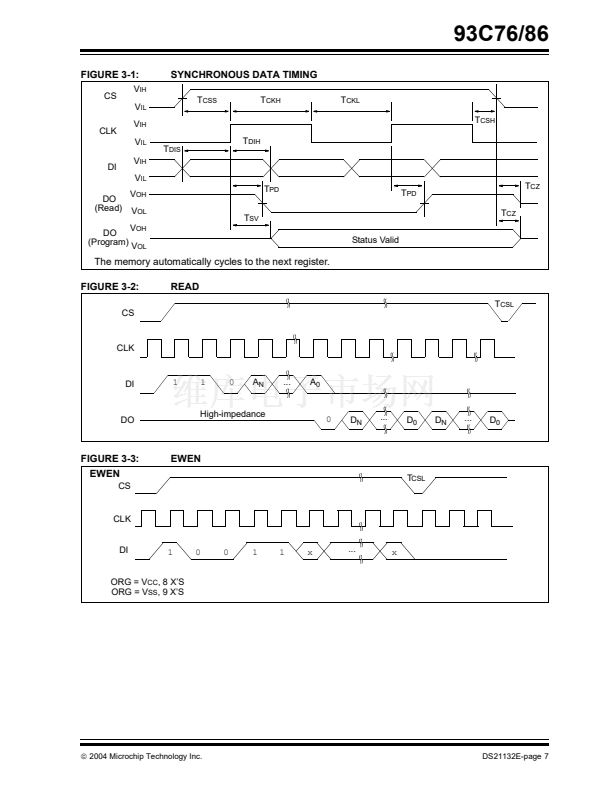
Read
3.4
Erase All (ERAL)
The
READ
instruction outputs the serial data of the
addressed memory location on the DO pin. A dummy
zero bit precedes the 16-bit (x16 organization) or 8-bit
(x8 organization) output string. The output data bits will
toggle on the rising edge of the CLK and are stable
after the specified time delay (T
PD
). Sequential read is
possible when CS is held high and clock transitions
continue. The memory address pointer will automati-
cally increment and output data sequentially.
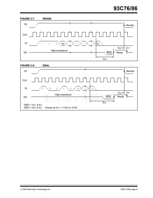
The
ERAL
instruction will erase the entire memory array
to the logical 鈥?鈥?state. The ERAL cycle is identical to
the erase cycle except for the different opcode. The
ERAL cycle is completely self-timed and commences
on the rising edge of the last address bit (A0). Note that
the Least Significant 8 or 9 address bits are "don鈥檛 care"
bits, depending on selection of x16 or x8 mode. Clock-
ing of the CLK pin is not necessary after the device has
entered the self clocking mode. The
ERAL
instruction is
ensured at Vcc = +4.5V to +5.5V.
The DO pin indicates the Ready/Busy status of the
device if the CS is high. The Ready/Busy status will be
displayed on the DO pin until the next Start bit is
received as long as CS is high. Bringing the CS low will
place the device in Standby mode and cause the DO
pin to enter the high-impedance state. DO at logical 鈥?鈥?/div>
indicates that programming is still in progress. DO at
logical 鈥?鈥?indicates that the entire device has been
erased and is ready for another instruction.
The ERAL cycle takes 15 ms maximum (8 ms typical).
3.2
Erase
The
ERASE
instruction forces all data bits of the
specified address to the logical 鈥?鈥?state. The self-timed
programming cycle is initiated on the rising edge of
CLK as the last address bit (A0) is clocked in. At this
point, the CLK, CS and DI inputs become 鈥渄on鈥檛 cares鈥?
The DO pin indicates the Ready/Busy status of the
device if the CS is high. The Ready/Busy status will be
displayed on the DO pin until the next Start bit is
received as long as CS is high. Bringing the CS low will
place the device in Standby mode and cause the DO
pin to enter the high-impedance state. DO at logical 鈥?鈥?/div>
indicates that programming is still in progress. DO at
logical 鈥?鈥?indicates that the register at the specified
address has been erased and the device is ready for
another instruction.
The erase cycle takes 3 ms per word (typical).
3.5
Write All (WRAL)
3.3
Write
The
WRITE
instruction is followed by 16 bits (or by 8
bits) of data to be written into the specified address.
The self-timed programming cycle is initiated on the
rising edge of CLK as the last data bit (D0) is clocked
in. At this point, the CLK, CS and DI inputs become
鈥渄on鈥檛 cares鈥?
The DO pin indicates the Ready/Busy status of the
device if the CS is high. The Ready/Busy status will be
displayed on the DO pin until the next Start bit is
received as long as CS is high. Bringing the CS low will
place the device in Standby mode and cause the DO
pin to enter the high-impedance state. DO at logical 鈥?鈥?/div>
indicates that programming is still in progress. DO at
logical 鈥?鈥?indicates that the register at the specified
address has been written and the device is ready for
another instruction.
The write cycle takes 3 ms per word (typical).
The
WRAL
instruction will write the entire memory array
with the data specified in the command. The WRAL
cycle is completely self-timed and commences on the
rising edge of the last address bit (A0). Note that the
Least Significant 8 or 9 address bits are 鈥渄on鈥檛 cares鈥?
depending on selection of x16 or x8 mode. Clocking of
the CLK pin is not necessary after the device has
entered the self clocking mode. The WRAL command
does include an automatic ERAL cycle for the device.
Therefore, the
WRAL
instruction does not require an
ERAL
instruction but the chip must be in the EWEN
status. The
WRAL
instruction is ensured at Vcc = +4.5V
to +5.5V.
The DO pin indicates the Ready/Busy status of the
device if the CS is high. The Ready/Busy status will be
displayed on the DO pin until the next Start bit is
received as long as CS is high. Bringing the CS low will
place the device in Standby mode and cause the DO
pin to enter the high-impedance state. DO at logical 鈥?鈥?/div>
indicates that programming is still in progress. DO at
logical 鈥?鈥?indicates that the entire device has been
written and is ready for another instruction.
The WRAL cycle takes 30 ms maximum (16 ms
typical).
DS21132E-page 6
铮?/div>
2004 Microchip Technology Inc.
93C86-E/P 产品属性
Microchip
电可擦除可编程只读存储器
16 Kbit
1 K x 16 or 2 K x 8
200 yr
2 MHz
3 mA
4.5 V, 5.5 V
+ 125 C
Through Hole
PDIP-8
3-Wire
- 40 C
Tube
60
5.5 V
4.5 V
93C86-E/P相关型号PDF文件下载
-
型号
版本
描述
厂商
下载
-
英文版
8K/16K 5.0V Microwire Serial EEPROM
-
英文版
8K/16K 5.0V Microwire Serial EEPROM
MICROCHIP ...
-
英文版
16K Microwire Compatible Serial EEPROM
-
英文版
1K-16K Microwire 串行EEPROM
-
英文版
16K Microwire Compatible Serial EEPROM
-
英文版
-
英文版
1K-16K Microwire 串行EEPROM
-
英文版
16K Microwire Compatible Serial EEPROM
-
英文版
1K-16K Microwire 串行EEPROM
-
英文版
8K/16K 5.0V Microwire Serial EEPROM
-
英文版
8K/16K 5.0V Microwire Serial EEPROM
MICROCHIP ...
-
英文版
Microwire Serial EEPROM
ETC
-
英文版
8K/16K 2.5V Microwire Serial EEPROM
-
英文版
8K/16K 5.0V Microwire Serial EEPROM
-
英文版
8K/16K 5.0V Microwire Serial EEPROM
MICROCHIP ...
-
英文版
8K/16K 5.0V Microwire Serial EEPROM
-
英文版
8K/16K 5.0V Microwire Serial EEPROM
MICROCHIP ...
-
英文版
8K/16K 5.0V Microwire Serial EEPROM
-
英文版
8K/16K 5.0V Microwire Serial EEPROM
MICROCHIP ...
-
英文版
Microwire Serial EEPROM
ETC


 1
1
 2
2
 3
3
 4
4
 5
5
 6
6
 7
7
 8
8
 9
9
 10
10
 11
11
 12
12
 13
13
 14
14
 15
15
 16
16
 17
17
 18
18
 19
19
 20
20
