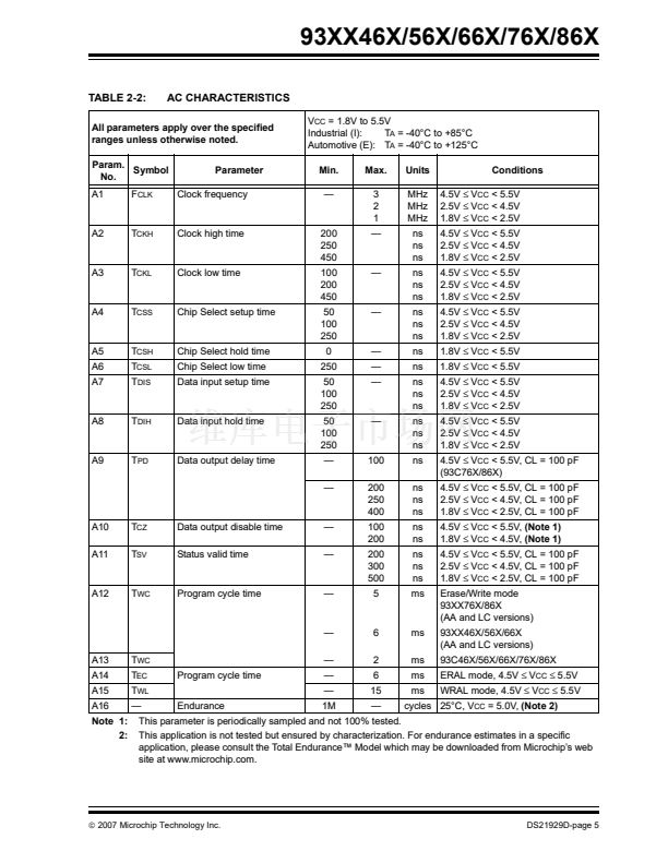
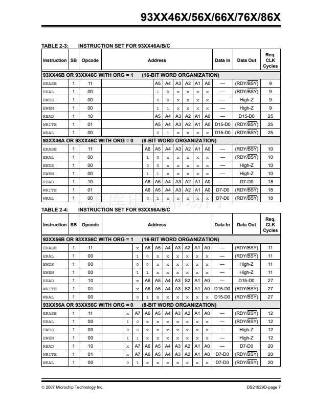
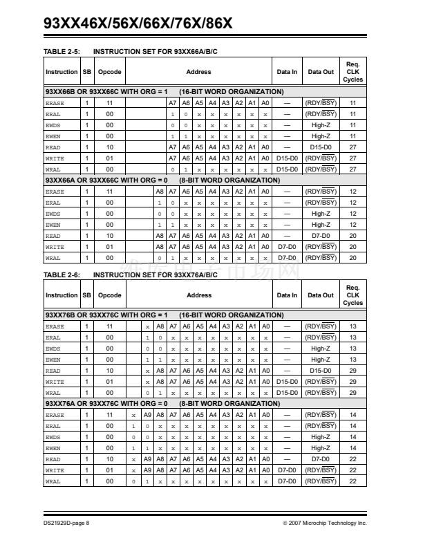
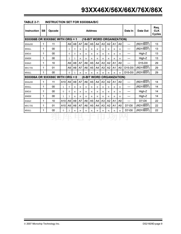
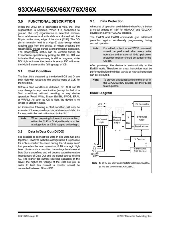
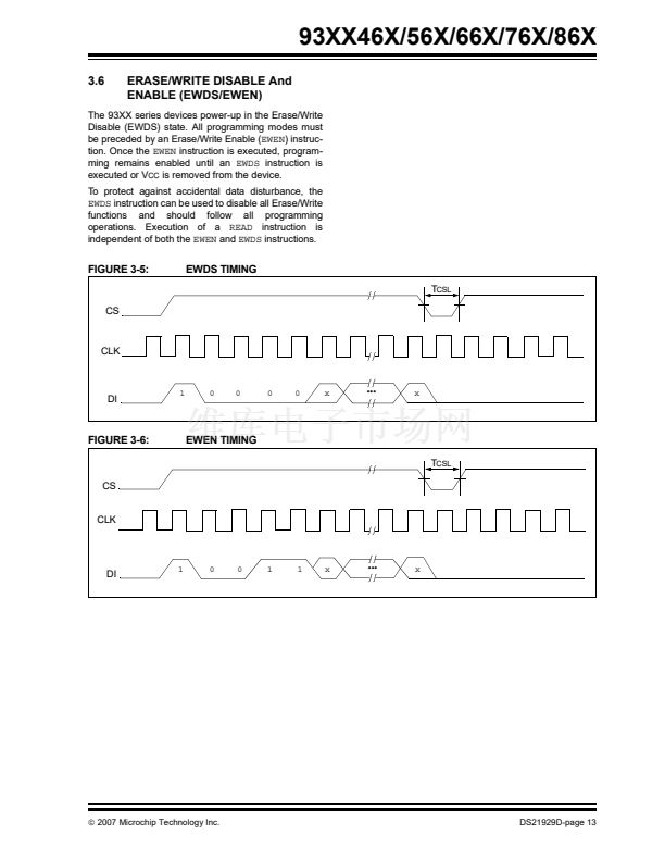
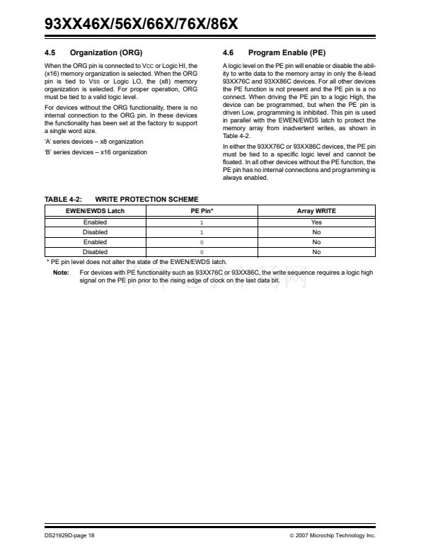
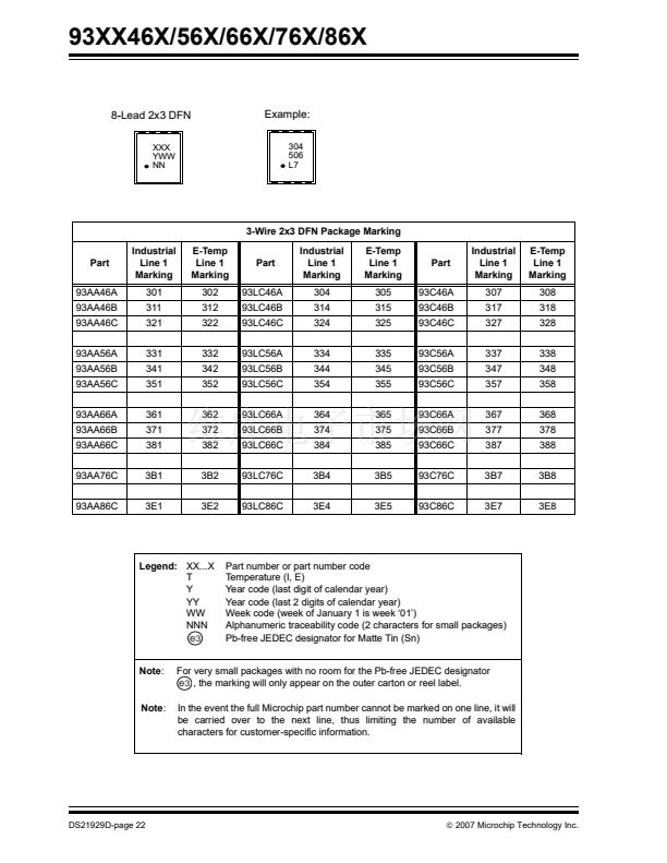
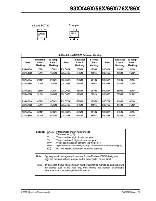
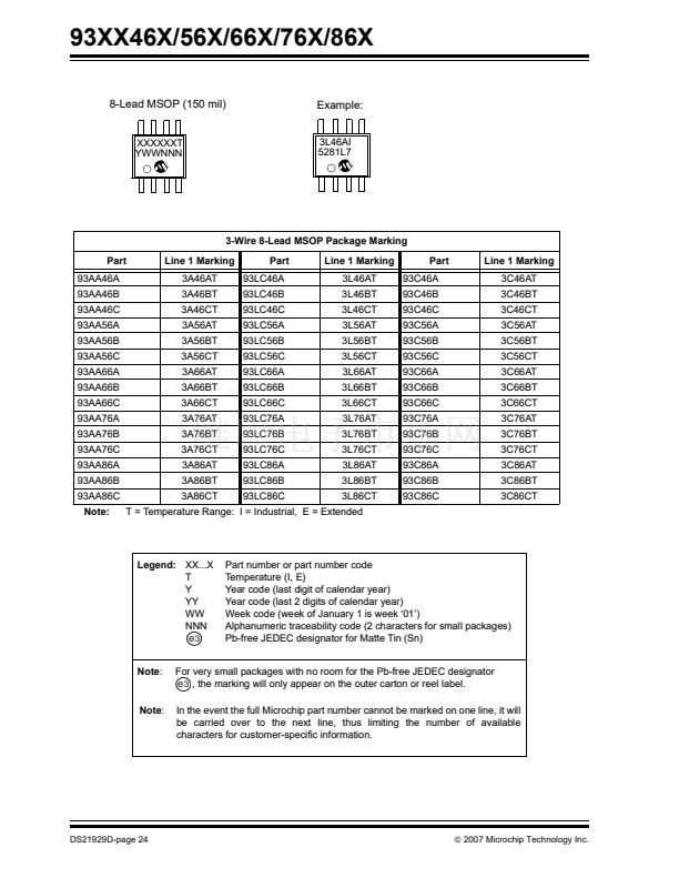
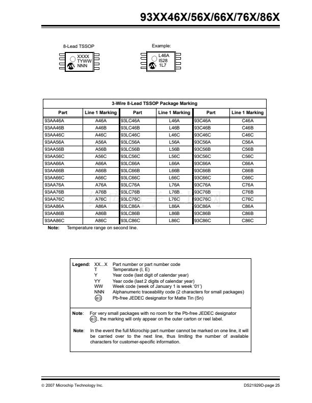
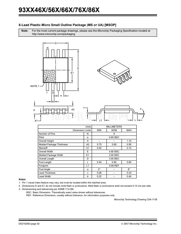
93XX46X/56X/66X/76X/86X
3.5
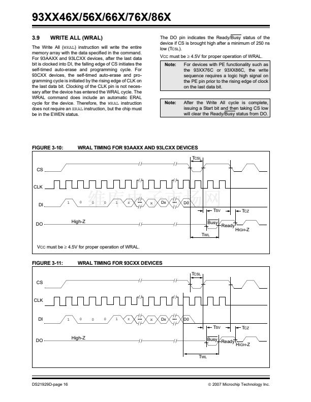
ERASE ALL (ERAL)
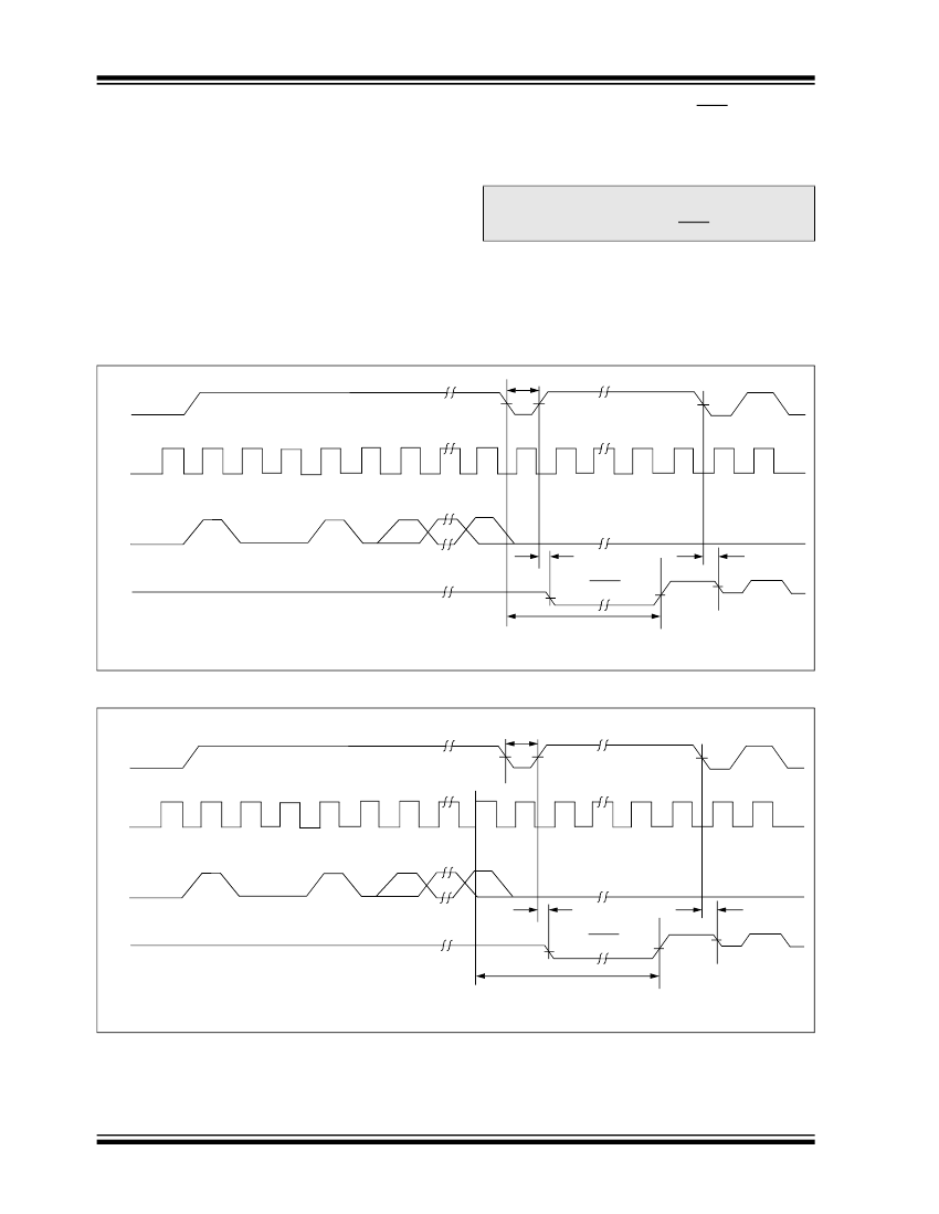
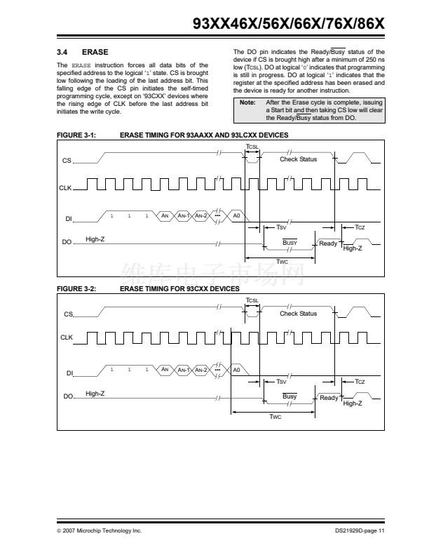
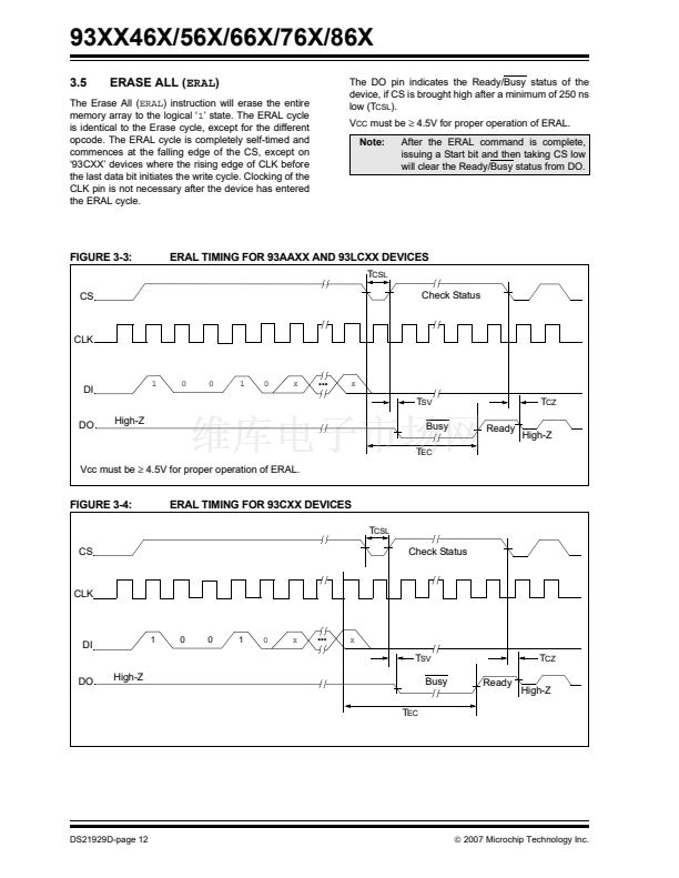
The Erase All (ERAL) instruction will erase the entire
memory array to the logical 鈥?鈥?state. The ERAL cycle
is identical to the Erase cycle, except for the different
opcode. The ERAL cycle is completely self-timed and
commences at the falling edge of the CS, except on
鈥?3CXX鈥?devices where the rising edge of CLK before
the last data bit initiates the write cycle. Clocking of the
CLK pin is not necessary after the device has entered
the ERAL cycle.
The DO pin indicates the Ready/Busy status of the
device, if CS is brought high after a minimum of 250 ns
low (T
CSL
).
V
CC
must be
鈮?/div>
4.5V for proper operation of ERAL.
Note:
After the ERAL command is complete,
issuing a Start bit and then taking CS low
will clear the Ready/Busy status from DO.
FIGURE 3-3:
ERAL TIMING FOR 93AAXX AND 93LCXX DEVICES
T
CSL
CS
Check Status
CLK
DI
High-Z
1
0
0
1
0
X
鈥⑩€⑩€?/div>
X
T
SV
DO
Busy
T
EC
Vcc must be
鈮?/div>
4.5V for proper operation of ERAL.
Ready
T
CZ
High-Z
FIGURE 3-4:
ERAL TIMING FOR 93CXX DEVICES
T
CSL
CS
Check Status
CLK
DI
High-Z
1
0
0
1
0
X
鈥⑩€⑩€?/div>
X
T
SV
DO
Busy
T
EC
Ready
T
CZ
High-Z
DS21929D-page 12
漏
2007 Microchip Technology Inc.


 1
1
 2
2
 3
3
 4
4
 5
5
 6
6
 7
7
 8
8
 9
9
 10
10
 11
11
 12
12
 13
13
 14
14
 15
15
 16
16
 17
17
 18
18
 19
19
 20
20
 21
21
 22
22
 23
23
 24
24
 25
25
 26
26
 27
27
 28
28
 29
29
 30
30
 31
31
 32
32
 33
33
 34
34
 35
35
 36
36
 37
37
 38
38
