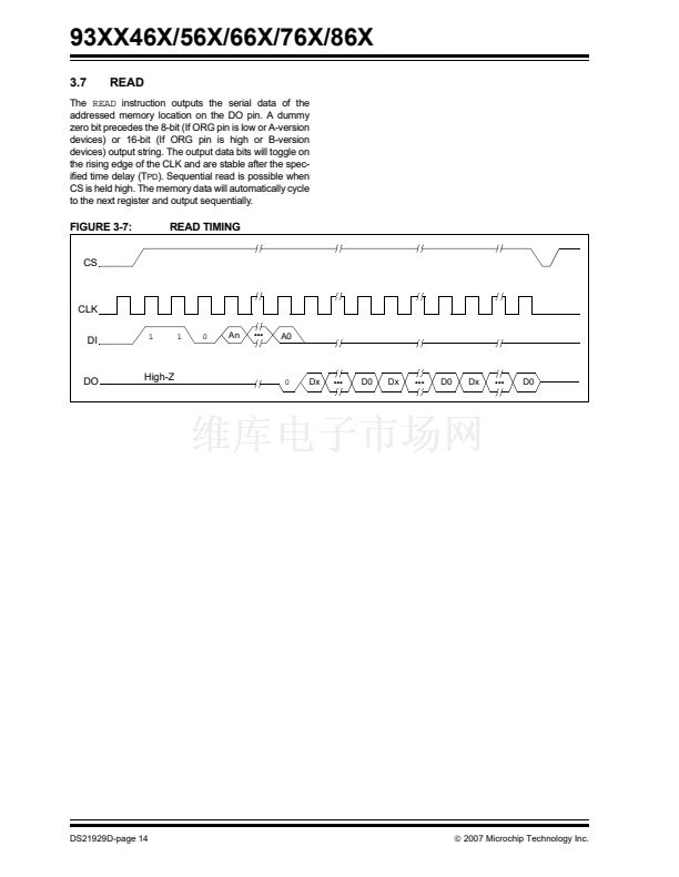
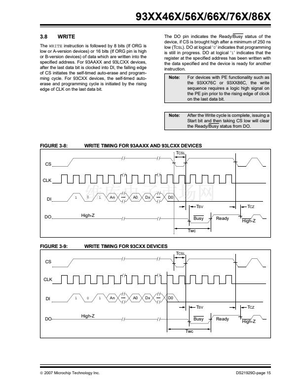
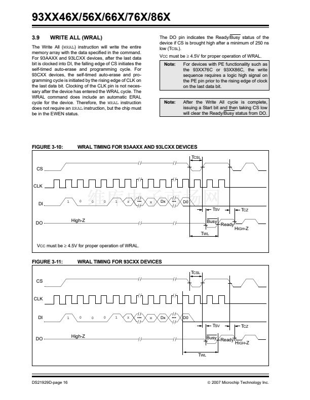
93XX46X/56X/66X/76X/86X
4.5
Organization (ORG)
4.6
Program Enable (PE)
When the ORG pin is connected to V
CC
or Logic HI, the
(x16) memory organization is selected. When the ORG
pin is tied to V
SS
or Logic LO, the (x8) memory
organization is selected. For proper operation, ORG
must be tied to a valid logic level.
For devices without the ORG functionality, there is no
internal connection to the ORG pin. In these devices
the functionality has been set at the factory to support
a single word size.
鈥楢鈥?series devices 鈥?x8 organization
鈥楤鈥?series devices 鈥?x16 organization
A logic level on the PE pin will enable or disable the abil-
ity to write data to the memory array in only the 8-lead
93XX76C and 93XX86C devices. For all other devices
the PE function is not present and the PE pin is a no
connect. When driving the PE pin to a logic High, the
device can be programmed, but when the PE pin is
driven Low, programming is inhibited. This pin is used
in parallel with the EWEN/EWDS latch to protect the
memory array from inadvertent writes, as shown in
Table 4-2.
In either the 93XX76C or 93XX86C devices, the PE pin
must be tied to a specific logic level and cannot be
floated. In all other devices without the PE function, the
PE pin has no internal connections and programming is
always enabled.
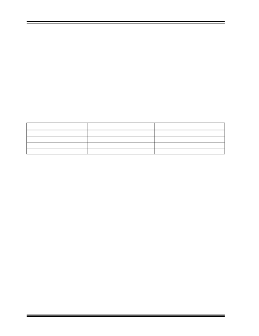
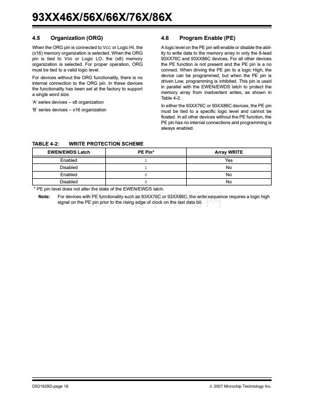
TABLE 4-2:
WRITE PROTECTION SCHEME
PE Pin*
1
1
0
0
Array WRITE
Yes
No
No
No
Enabled
Disabled
Enabled
Disabled
EWEN/EWDS Latch
* PE pin level does not alter the state of the EWEN/EWDS latch.
Note:
For devices with PE functionality such as 93XX76C or 93XX86C, the write sequence requires a logic high
signal on the PE pin prior to the rising edge of clock on the last data bit.
DS21929D-page 18
漏
2007 Microchip Technology Inc.


 1
1
 2
2
 3
3
 4
4
 5
5
 6
6
 7
7
 8
8
 9
9
 10
10
 11
11
 12
12
 13
13
 14
14
 15
15
 16
16
 17
17
 18
18
 19
19
 20
20
 21
21
 22
22
 23
23
 24
24
 25
25
 26
26
 27
27
 28
28
 29
29
 30
30
 31
31
 32
32
 33
33
 34
34
 35
35
 36
36
 37
37
 38
38
