CA3240, CA3240A
Absolute Maximum Ratings
Supply Voltage (Between V+ and V-) . . . . . . . . . . . . . . . . . . . . 36V
Differential Input Voltage . . . . . . . . . . . . . . . . . . . . . . . . . . . . . . . 8V
Input Voltage . . . . . . . . . . . . . . . . . . . . . . . . . (V+ +8V) to (V- -0.5V)
Input Current . . . . . . . . . . . . . . . . . . . . . . . . . . . . . . . . . . . . . . . 1mA
Output Short Circuit Duration (Note 1). . . . . . . . . . . . . . . . Indefinite
Thermal Information
Thermal Resistance (Typical, Note 2)
胃
JA
(
o
C/W)
8 Lead PDIP Package* . . . . . . . . . . . . . . . . . . . . . .
100
Maximum Junction Temperature (Plastic Package) . . . . . . . 150
o
C
Maximum Storage Temperature Range . . . . . . . . . -65
o
C to 150
o
C
Maximum Lead Temperature (Soldering 10s) . . . . . . . . . . . . 300
o
C
*Pb-free PDIPs can be used for through hole wave solder process-
ing only. They are not intended for use in Reflow solder processing
applications.
Operating Conditions
Temperature Range. . . . . . . . . . . . . . . . . . . . . . . . . . -40
o
C to 85
o
C
Voltage Range . . . . . . . . . . . . . . . . . . . . . 4V to 36V or
卤2V
to
卤18V
CAUTION: Stresses above those listed in 鈥淎bsolute Maximum Ratings鈥?may cause permanent damage to the device. This is a stress only rating and operation of the
device at these or any other conditions above those indicated in the operational sections of this specification is not implied.
NOTES:
1. Short circuit may be applied to ground or to either supply. Temperatures and/or supply voltages must be limited to keep dissipation within max-
imum rating.
2.
胃
JA
is measured with the component mounted on an evaluation PC board in free air.
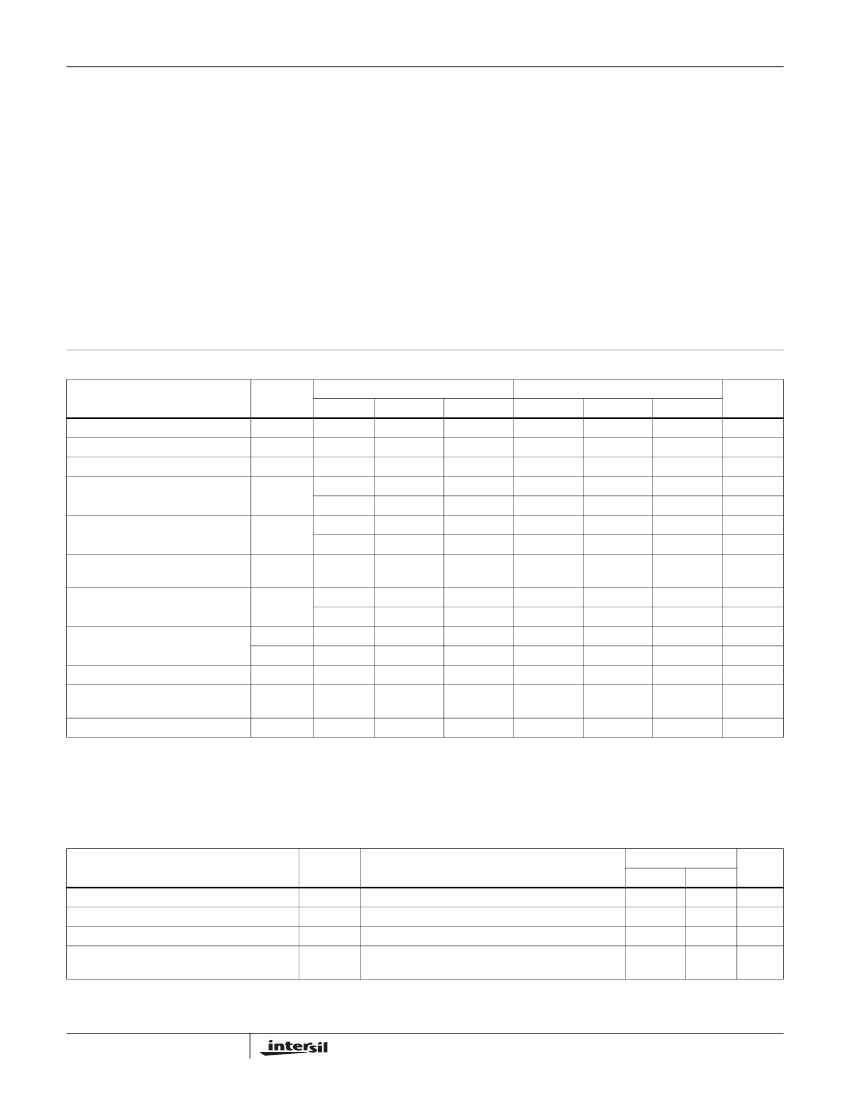
Electrical Specifications
PARAMETER
Input Offset Voltage
Input Offset Current
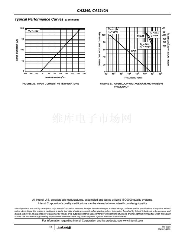
Input Current
Large-Signal Voltage Gain
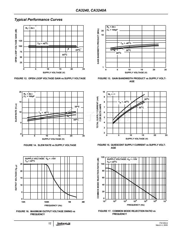
(See Figures 12, 27) (Note 3)
Common Mode Rejection
Ratio (See Figure 17)
For Equipment Design, V
SUPPLY
=
卤15V,
T
A
= 25
o
C, Unless Otherwise Specified
CA3240
SYMBOL
V
IO
I
IO
I
I
A
OL
CMRR
MIN
-
-
-
20
86
-
70
V
ICR
PSRR
(鈭哣
IO
/鈭哣卤)
V
OM
+
V
OM
-
V
OM-
I+
P
D
-15
-
76
12
-14
0.4
-
-
TYP
5
0.5
10
100
100
32
90
-15.5 to
+12.5
100
80
13
-14.4
0.13
8
240
MAX
15
30
50
-
-
320
-
11
150
-
-
-
-
12
360
MIN
-
-
-
20
86
-
70
-15
-
76
12
-14
0.4
-
-
CA3240A
TYP
2
0.5
10
100
100
32
90
-15.5 to
+12.5
100
80
13
-14.4
0.13
8
240
MAX
5
20
40
-
-
320
-
12
150
-
-
-
-
12
360
UNITS
mV
pA
pA
kV/V
dB
碌V/V
dB
V
碌V/V
dB
V
V
V
mA
mW
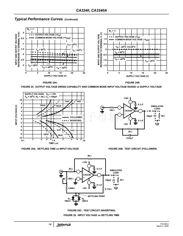
Common Mode Input Voltage Range
(See Figure24)
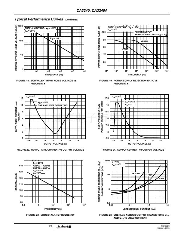
Power Supply Rejection Ratio
(See Figure 19)
Maximum Output Voltage (Note 4)
(See Figures 23, 24)
Maximum Output Voltage (Note 5)
Total Supply Current
(See Figure 15) For Both Amps
Total Device Dissipation
NOTES:
3. At V
O
= 26V
P-P
, +12V, -14V and R
L
= 2k鈩?
4. At R
L
= 2k鈩?
5. At V+ = 5V, V- = GND, I
SINK
= 200碌A.
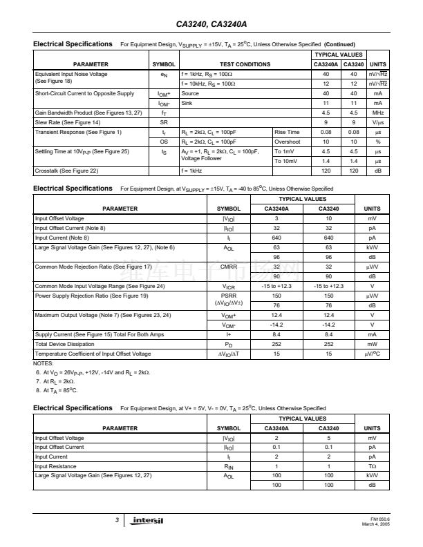
Electrical Specifications
PARAMETER
Input Resistance
Input Capacitance
Output Resistance
For Equipment Design, V
SUPPLY
=
卤15V,
T
A
= 25
o
C, Unless Otherwise Specified
TYPICAL VALUES
SYMBOL
R
I
C
I
R
O
e
N
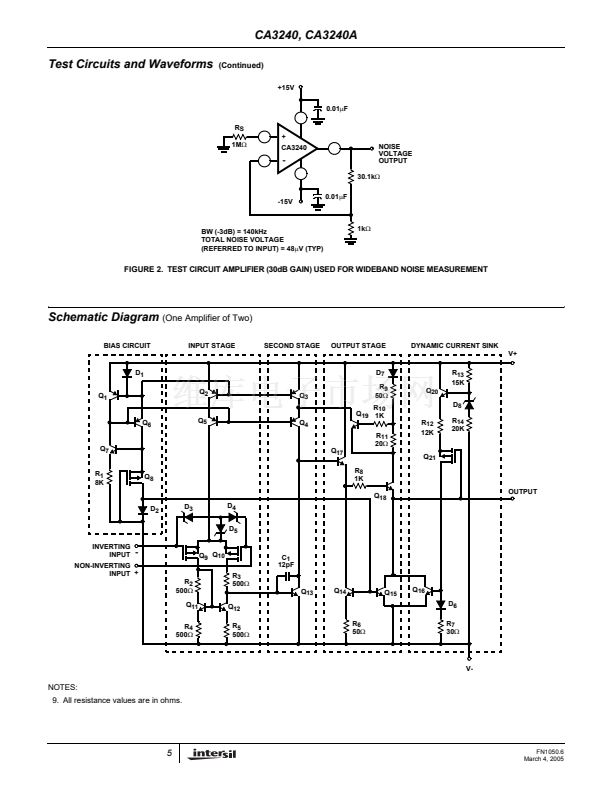
BW = 140kHz, R
S
= 1M鈩?/div>
TEST CONDITIONS
CA3240A CA3240
1.5
4
60
48
1.5
4
60
48
UNITS
T鈩?/div>
pF
鈩?/div>
碌V
Equivalent Wideband Input Noise Voltage
(See Figure 2)
2
FN1050.6
March 4, 2005


 1
1
 2
2
 3
3
 4
4
 5
5
 6
6
 7
7
 8
8
 9
9
 10
10
 11
11
 12
12
 13
13
 14
14
 15
15
