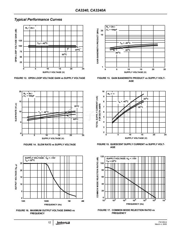
CA3240, CA3240A
Application Information
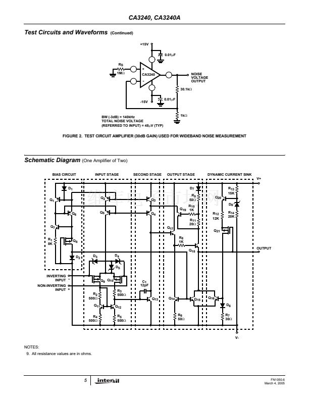
Circuit Description
The schematic diagram details one amplifier section of the
CA3240. It consists of a differential amplifier stage using PMOS
transistors (Q
9
and Q
10
) with gate-to-source protection against
static discharge damage provided by zener diodes D
3
, D
4
, and
D
5
. Constant current bias is applied to the differential amplifier
from transistors Q
2
and Q
5
connected as a constant current
source. This assures a high common-mode rejection ratio. The
output of the differential amplifier is coupled to the base of gain
stage transistor Q
13
by means of an NPN current mirror that
supplies the required differential-to-single-ended conversion.
The gain stage transistor Q
13
has a high impedance active
load (Q
3
and Q
4
) to provide maximum open-loop gain. The
collector of Q
13
directly drives the base of the compound
emitter-follower output stage. Pulldown for the output stage is
provided by two independent circuits: (1) constant-current-
connected transistors Q
14
and Q
15
and (2) dynamic current-
sink transistor Q
16
and its associated circuitry.
The level of
pulldown current is constant at about 1mA for Q
15
and varies
from 0 to 18mA for Q
16
depending on the magnitude of the
voltage between the output terminal and V+.
The dynamic
current sink becomes active whenever the output terminal is
more negative than V+ by about 15V. When this condition
exists, transistors Q
21
and Q
16
are turned on causing Q
16
to
sink current from the output terminal to V-. This current always
flows when the output is in the linear region, either from the
load resistor or from the emitter of Q
18
if no load resistor is
present. The purpose of this dynamic sink is to permit the
output to go within 0.2V (V
CE
(sat)) of V- with a 2k鈩?load to
ground.
When the load is returned to V+, it may be necessary
to supplement the 1mA of current from Q
15
in order to turn on
the dynamic current sink (Q
16
).
This may be accomplished by
placing a resistor (Approx. 2k鈩? between the output and V-.
Input Circuit Considerations
As indicated by the typical VICR, this device will accept
inputs as low as 0.5V below V-. However, a series current-
limiting resistor is recommended to limit the maximum input
terminal current to less than 1mA to prevent damage to the
input protection circuitry.
Moreover, some current-limiting resistance should be
provided between the inverting input and the output when
the CA3240 is used as a unity-gain voltage follower. This
resistance prevents the possibility of extremely large input-
signal transients from forcing a signal through the input-
protection network and directly driving the internal constant-
current source which could result in positive feedback via the
output terminal. A 3.9k鈩?resistor is sufficient.
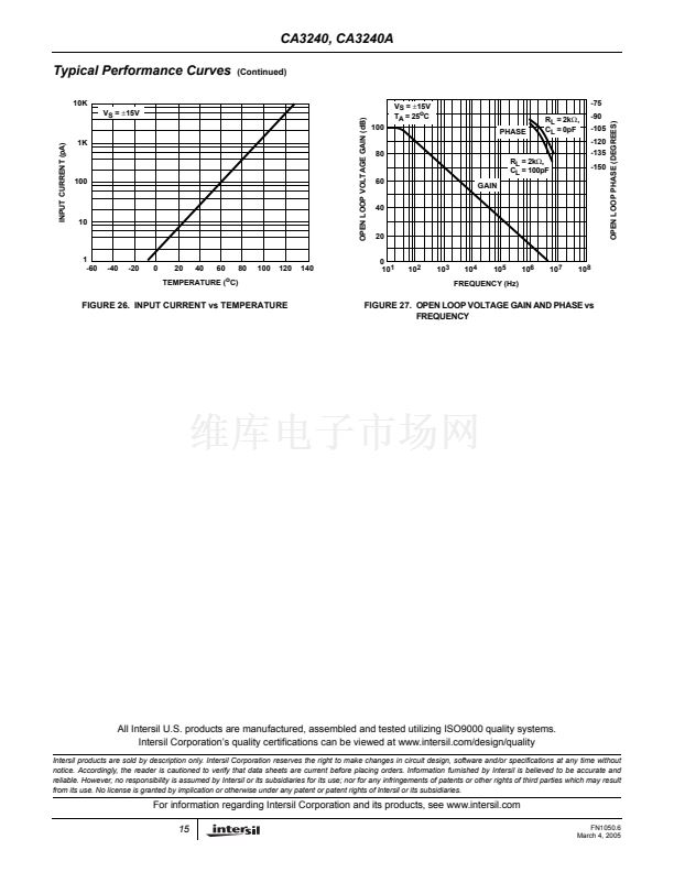
The typical input current is on the order of 10pA when the
inputs are centered at nominal device dissipation. As the
output supplies load current, device dissipation will increase,
raising the chip temperature and resulting in increased input
current. Figure 4 shows typical input-terminal current versus
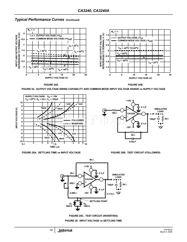
ambient temperature for the CA3240.
V+
+HV
LOAD
CA3240
R
L
R
S
120V
AC
LOAD
30V NO LOAD
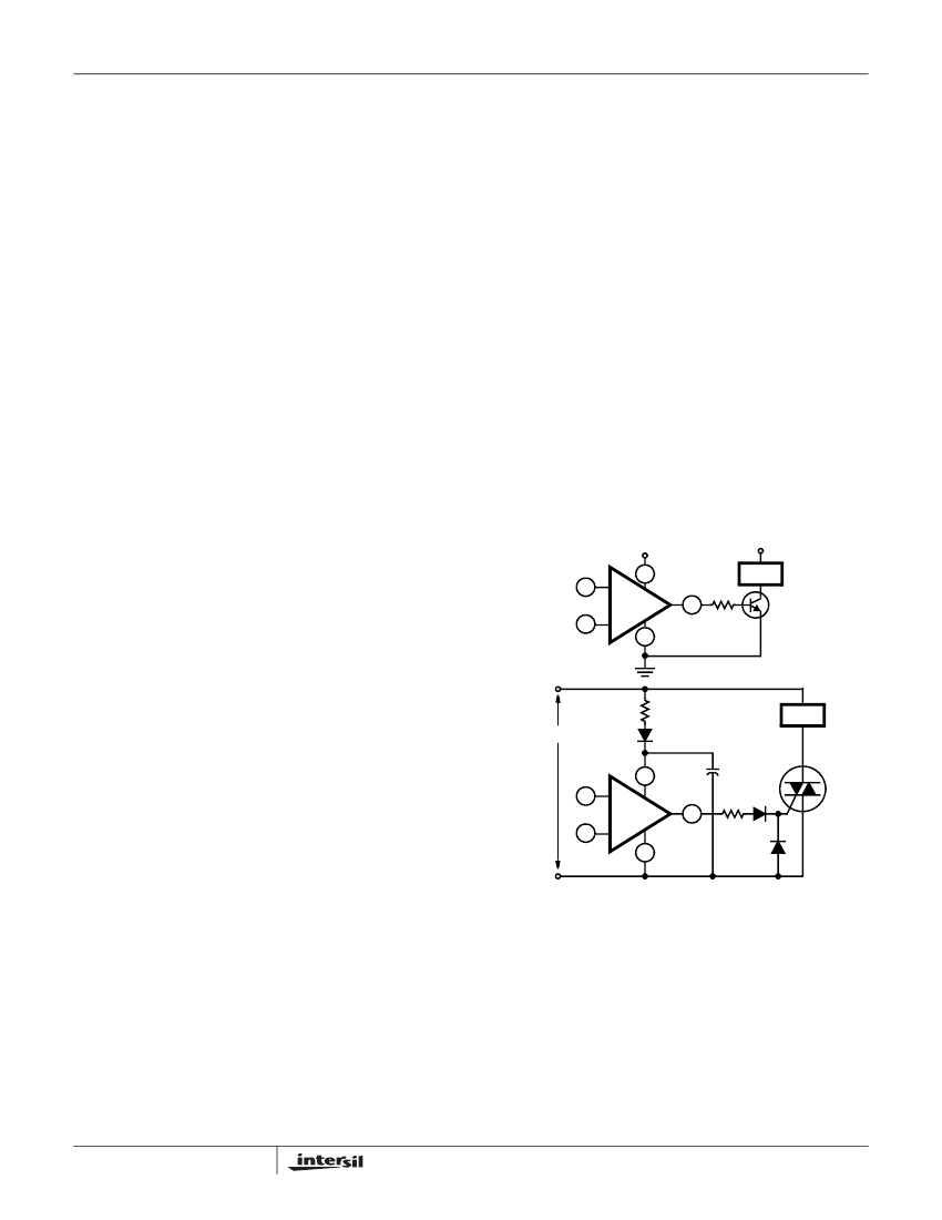
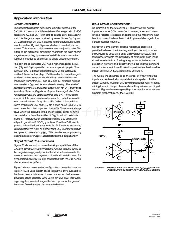
Output Circuit Considerations
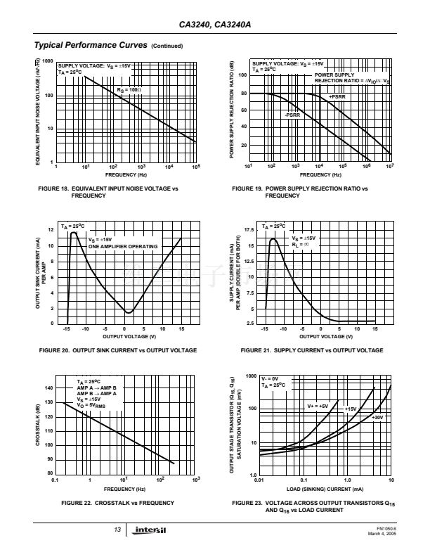
Figure 23 shows output current-sinking capabilities of the
CA3240 at various supply voltages. Output voltage swing to
the negative supply rail permits this device to operate both
power transistors and thyristors directly without the need for
level-shifting circuitry usually associated with the 741 series
of operational amplifiers.
Figure 3 shows some typical configurations. Note that a series
resistor, RL, is used in both cases to limit the drive available to
the driven device. Moreover, it is recommended that a series
diode and shunt diode be used at the thyristor input to prevent
large negative transient surges that can appear at the gate of
thyristors, from damaging the integrated circuit.
MT
2
CA3240
R
L
MT
1
FIGURE 3. METHODS OF UTILIZING THE V
CE (SAT)
SINKING
CURRENT CAPABILITY OF THE CA3240 SERIES
6
FN1050.6
March 4, 2005


 1
1
 2
2
 3
3
 4
4
 5
5
 6
6
 7
7
 8
8
 9
9
 10
10
 11
11
 12
12
 13
13
 14
14
 15
15
