= 100鈩?/div>
Source
Sink
CA3240A CA3240
40
12
40
11
4.5
9
0.08
10
4.5
1.4
120
40
12
40
11
4.5
9
0.08
10
4.5
1.4
120
UNITS
nV/鈭欻z
nV/鈭欻z
mA
mA
MHz
V/碌s
碌s
%
碌s
碌s
dB
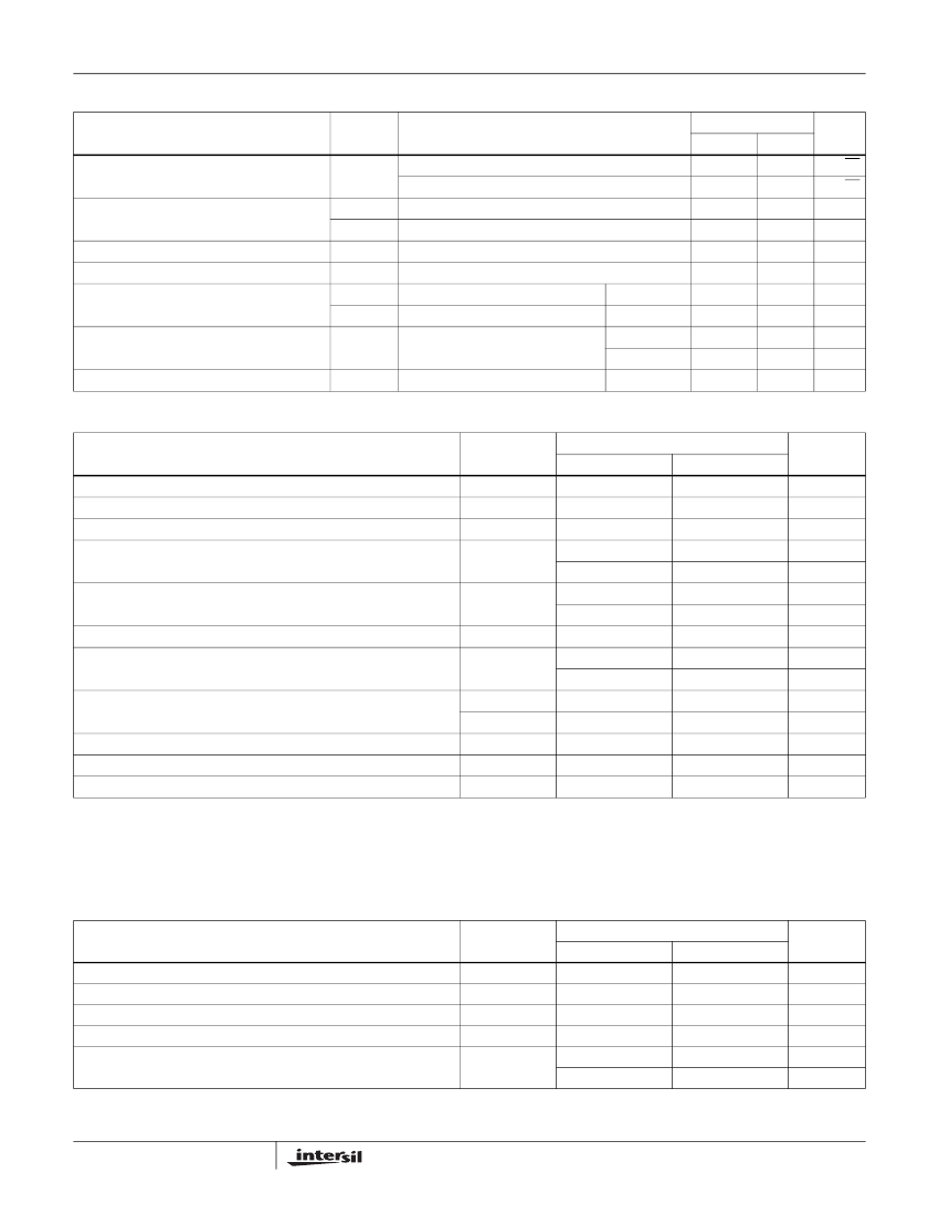
Electrical Specifications
For Equipment Design, at V
SUPPLY
=
卤15V,
T
A
= -40 to 85
o
C, Unless Otherwise Specified
TYPICAL VALUES
PARAMETER
Input Offset Voltage
Input Offset Current (Note 8)
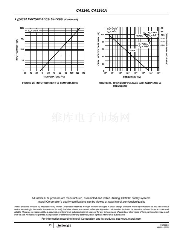
Input Current (Note 8)
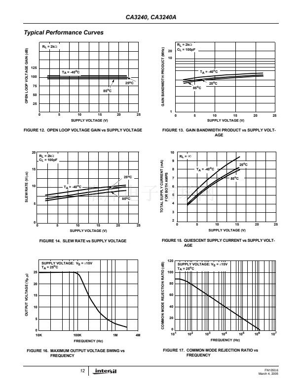
Large Signal Voltage Gain (See Figures 12, 27), (Note 6)
SYMBOL
|V
IO
|
|I
IO
|
I
I
A
OL
CMRR
CA3240A
3
32
640
63
96
CA3240
10
32
640
63
96
32
90
-15 to +12.3
150
76
12.4
-14.2
8.4
252
15
UNITS
mV
pA
pA
kV/V
dB
碌V/V
dB
V
碌V/V
dB
V
V
mA
mW
碌V/
o
C
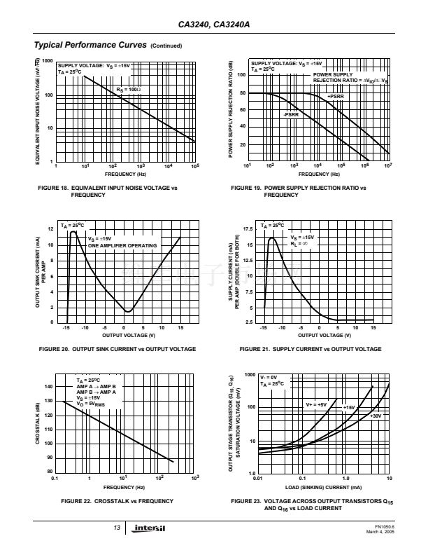
Common Mode Rejection Ratio (See Figure 17)
32
90
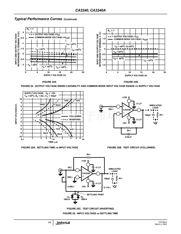
Common Mode Input Voltage Range (See Figure 24)
Power Supply Rejection Ratio (See Figure 19)
V
ICR
PSRR
(鈭哣
IO
/鈭哣卤)
V
OM
+
V
OM
-
I+
P
D
鈭哣
IO
/鈭員
-15 to +12.3
150
76
12.4
-14.2
8.4
252
15
Maximum Output Voltage (Note 7) (See Figures 23, 24)
Supply Current (See Figure 15) Total For Both Amps
Total Device Dissipation
Temperature Coefficient of Input Offset Voltage
NOTES:
6. At V
O
= 26V
P-P
, +12V, -14V and R
L
= 2k鈩?
7. At R
L
= 2k鈩?
8. At T
A
= 85
o
C.
Electrical Specifications
For Equipment Design, at V+ = 5V, V- = 0V, T
A
= 25
o
C, Unless Otherwise Specified
TYPICAL VALUES
PARAMETER
Input Offset Voltage
Input Offset Current
Input Current
Input Resistance
Large Signal Voltage Gain (See Figures 12, 27)
SYMBOL
|V
IO
|
|I
IO
|
I
I
R
IN
A
OL
CA3240A
2
0.1
2
1
100
100
CA3240
5
0.1
2
1
100
100
UNITS
mV
pA
pA
T鈩?/div>
kV/V
dB
3
FN1050.6
March 4, 2005


 1
1
 2
2
 3
3
 4
4
 5
5
 6
6
 7
7
 8
8
 9
9
 10
10
 11
11
 12
12
 13
13
 14
14
 15
15
