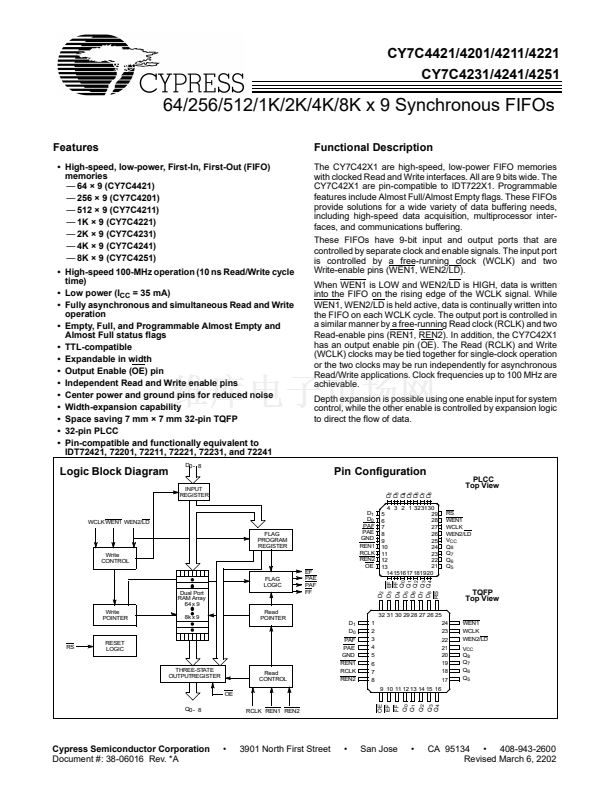
CY7C4421/4201/4211/4221
CY7C4231/4241/4251
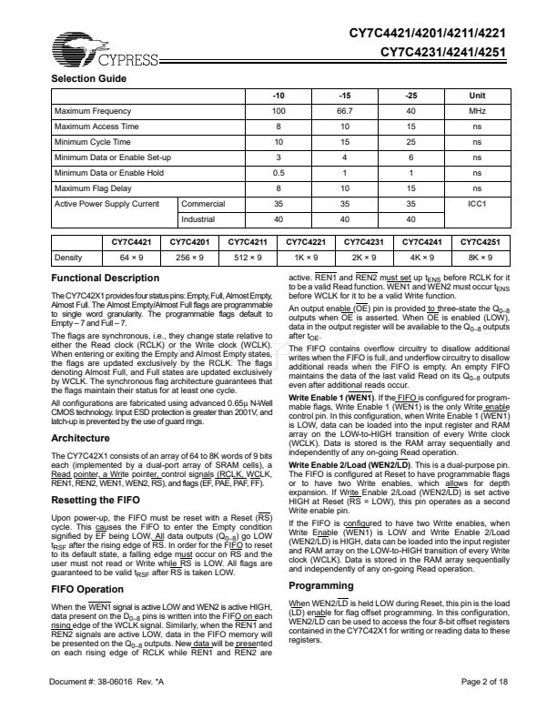
Selection Guide
-10
Maximum Frequency
Maximum Access Time
Minimum Cycle Time
Minimum Data or Enable Set-up
Minimum Data or Enable Hold
Maximum Flag Delay
Active Power Supply Current
Commercial
Industrial
CY7C4421
Density
64 脳 9
CY7C4201
256 脳 9
CY7C4211
512 脳 9
100
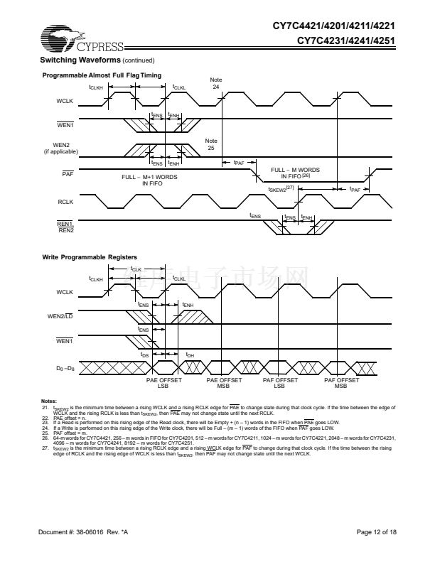
8
10
3
0.5
8
35
40
CY7C4221
1K 脳 9
-15
66.7
10
15
4
1
10
35
40
CY7C4231
2K 脳 9
-25
40
15
25
6
1
15
35
40
CY7C4241
4K 脳 9
CY7C4251
8K 脳 9
Unit
MHz
ns
ns
ns
ns
ns
ICC1
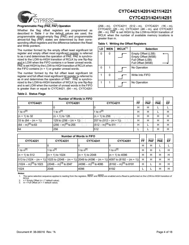
Functional Description
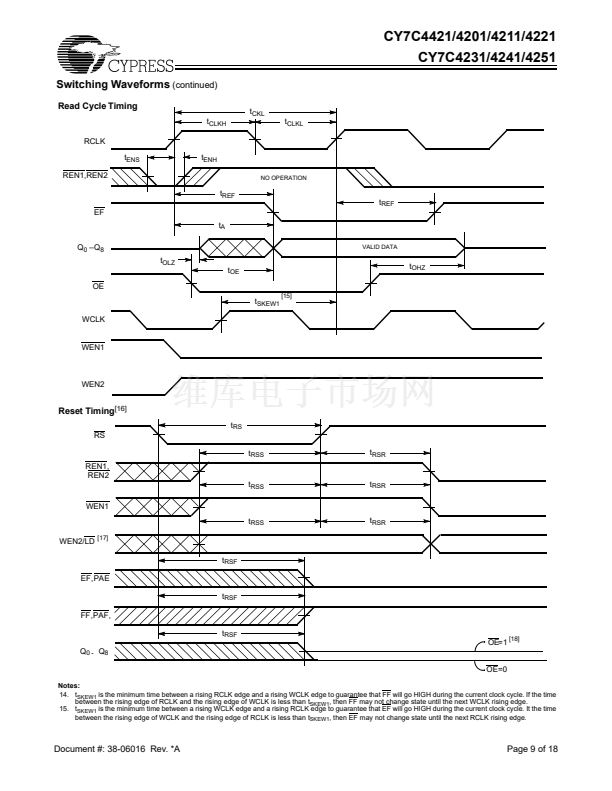
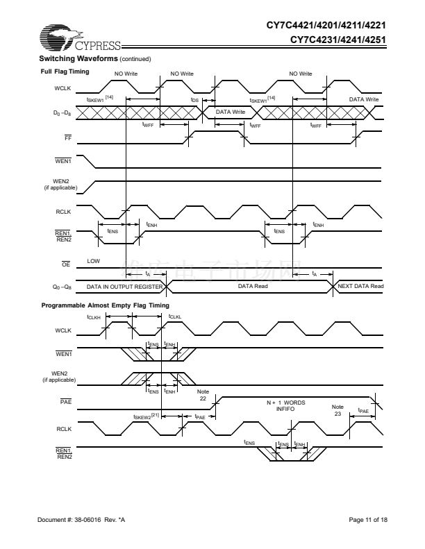
The CY7C42X1 provides four status pins: Empty, Full, Almost Empty,
Almost Full. The Almost Empty/Almost Full flags are programmable
to single word granularity. The programmable flags default to
Empty 鈥?7 and Full 鈥?7.
The flags are synchronous, i.e., they change state relative to
either the Read clock (RCLK) or the Write clock (WCLK).
When entering or exiting the Empty and Almost Empty states,
the flags are updated exclusively by the RCLK. The flags
denoting Almost Full, and Full states are updated exclusively
by WCLK. The synchronous flag architecture guarantees that
the flags maintain their status for at least one cycle.
All configurations are fabricated using advanced 0.65碌 N-Well
CMOS technology. Input ESD protection is greater than 2001V, and
latch-up is prevented by the use of guard rings.
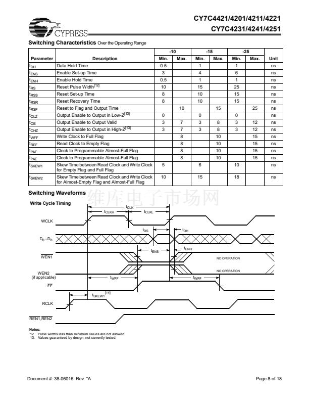
active. REN1 and REN2 must set up t
ENS
before RCLK for it
to be a valid Read function. WEN1 and WEN2 must occur t
ENS
before WCLK for it to be a valid Write function.
An output enable (OE) pin is provided to three-state the Q
0鈥?
outputs when OE is asserted. When OE is enabled (LOW),
data in the output register will be available to the Q
0鈥?
outputs
after t
OE
.
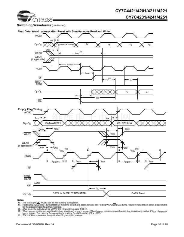
The FIFO contains overflow circuitry to disallow additional
writes when the FIFO is full, and underflow circuitry to disallow
additional reads when the FIFO is empty. An empty FIFO
maintains the data of the last valid Read on its Q
0鈥?
outputs
even after additional reads occur.
Write Enable 1 (WEN1).
If the FIFO is configured for program-
mable flags, Write Enable 1 (WEN1) is the only Write enable
control pin. In this configuration, when Write Enable 1 (WEN1)
is LOW, data can be loaded into the input register and RAM
array on the LOW-to-HIGH transition of every Write clock
(WCLK). Data is stored is the RAM array sequentially and
independently of any on-going Read operation.
Write Enable 2/Load (WEN2/LD).
This is a dual-purpose pin.
The FIFO is configured at Reset to have programmable flags
or to have two Write enables, which allows for depth
expansion. If Write Enable 2/Load (WEN2/LD) is set active
HIGH at Reset (RS = LOW), this pin operates as a second
Write enable pin.
If the FIFO is configured to have two Write enables, when
Write Enable (WEN1) is LOW and Write Enable 2/Load
(WEN2/LD) is HIGH, data can be loaded into the input register
and RAM array on the LOW-to-HIGH transition of every Write
clock (WCLK). Data is stored in the RAM array sequentially
and independently of any on-going Read operation.
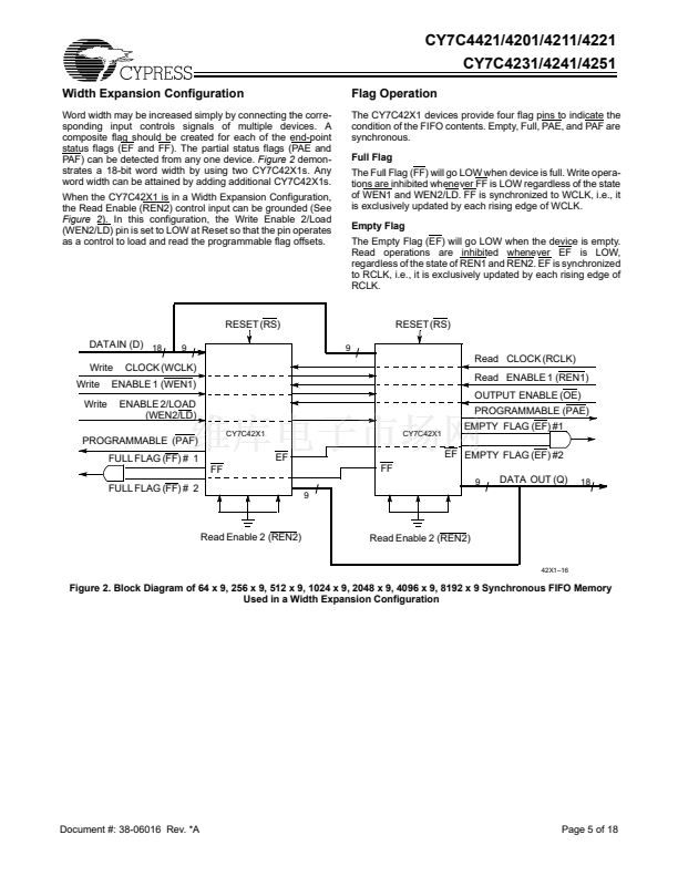
Architecture
The CY7C42X1 consists of an array of 64 to 8K words of 9 bits
each (implemented by a dual-port array of SRAM cells), a
Read pointer, a Write pointer, control signals (RCLK, WCLK,
REN1, REN2, WEN1, WEN2, RS), and flags (EF, PAE, PAF, FF).
Resetting the FIFO
Upon power-up, the FIFO must be reset with a Reset (RS)
cycle. This causes the FIFO to enter the Empty condition
signified by EF being LOW. All data outputs (Q
0鈥?
) go LOW
t
RSF
after the rising edge of RS. In order for the FIFO to reset
to its default state, a falling edge must occur on RS and the
user must not read or Write while RS is LOW. All flags are
guaranteed to be valid t
RSF
after RS is taken LOW.
FIFO Operation
When the WEN1 signal is active LOW and WEN2 is active HIGH,
data present on the D
0鈥?
pins is written into the FIFO on each
rising edge of the WCLK signal. Similarly, when the REN1 and
REN2 signals are active LOW, data in the FIFO memory will
be presented on the Q
0鈥?
outputs. New data will be presented
on each rising edge of RCLK while REN1 and REN2 are
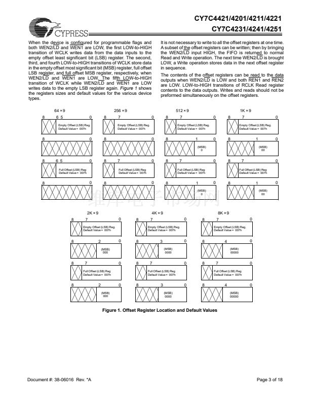
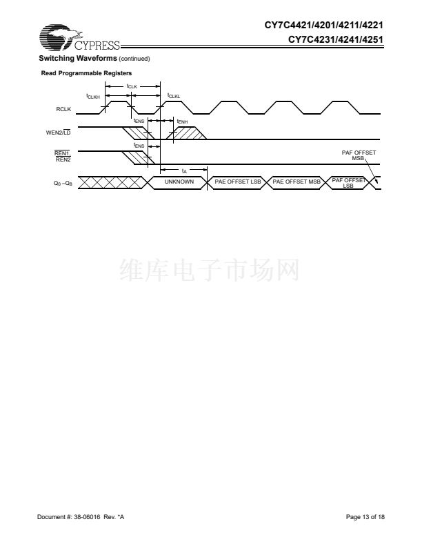
Programming
When WEN2/LD is held LOW during Reset, this pin is the load
(LD) enable for flag offset programming. In this configuration,
WEN2/LD can be used to access the four 8-bit offset registers
contained in the CY7C42X1 for writing or reading data to these
registers.
Document #: 38-06016 Rev. *A
Page 2 of 18


 1
1
 2
2
 3
3
 4
4
 5
5
 6
6
 7
7
 8
8
 9
9
 10
10
 11
11
 12
12
 13
13
 14
14
 15
15
 16
16
 17
17
 18
18
