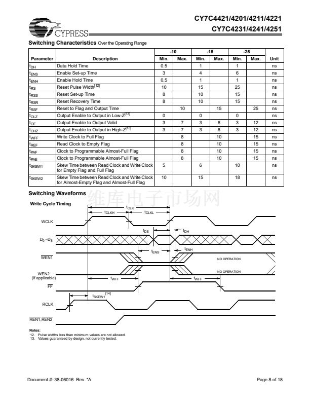
CY7C4421/4201/4211/4221
CY7C4231/4241/4251
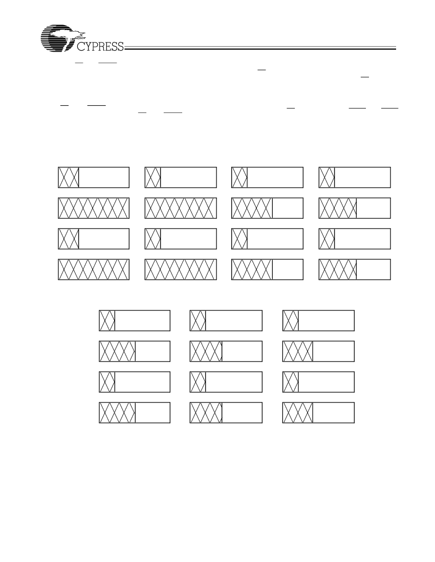
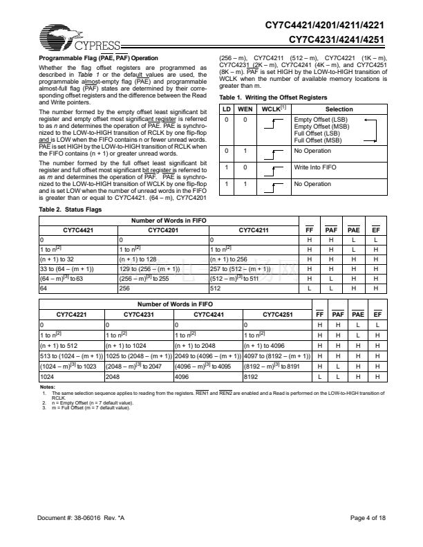
When the device is configured for programmable flags and
both WEN2/LD and WEN1 are LOW, the first LOW-to-HIGH
transition of WCLK writes data from the data inputs to the
empty offset least significant bit (LSB) register. The second,
third, and fourth LOW-to-HIGH transitions of WCLK store data
in the empty offset most significant bit (MSB) register, full offset
LSB register, and full offset MSB register, respectively, when
WEN2/LD and WEN1 are LOW. The fifth LOW-to-HIGH
transition of WCLK while WEN2/LD and WEN1 are LOW
writes data to the empty LSB register again.
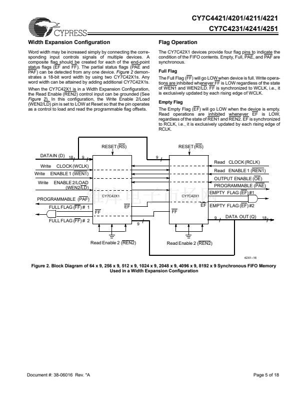
Figure 1
shows
the registers sizes and default values for the various device
types.
64 脳 9
8
6 5
0
8
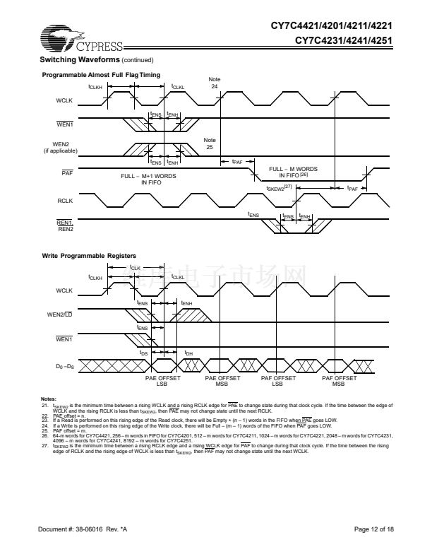
256 脳 9
7
Empty Offset (LSB) Reg.
Default Value = 007h
It is not necessary to write to all the offset registers at one time.
A subset of the offset registers can be written; then by bringing
the WEN2/LD input HIGH, the FIFO is returned to normal
Read and Write operation. The next time WEN2/LD is brought
LOW, a Write operation stores data in the next offset register
in sequence.
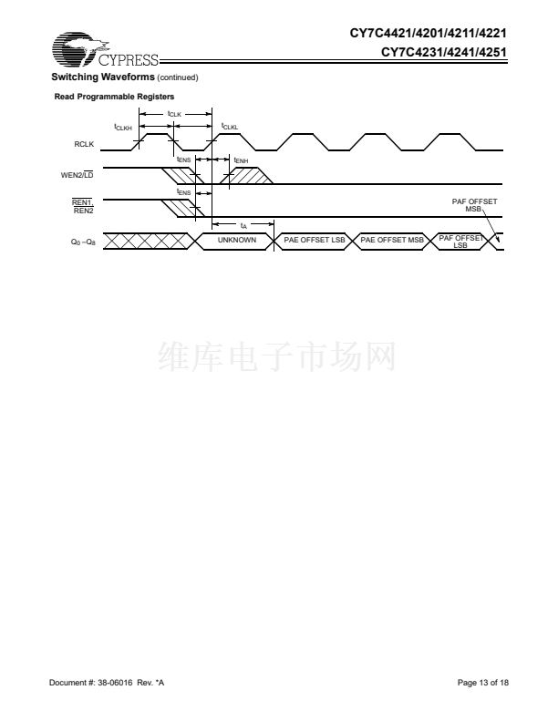
The contents of the offset registers can be read to the data
outputs when WEN2/LD is LOW and both REN1 and REN2
are LOW. LOW-to-HIGH transitions of RCLK Read register
contents to the data outputs. Writes and reads should not be
preformed simultaneously on the offset registers.
512 脳 9
0
8
7
Empty Offset (LSB) Reg.
Default Value = 007h
1K 脳 9
0
8
7
Empty Offset (LSB) Reg.
Default Value = 007h
0
Empty Offset (LSB) Reg.
Default Value = 007h
8
0
8
0
8
1
(MSB)
0
0
8
1
(MSB)
00
0
8
6 5
Full Offset (LSB) Reg
Default Value = 007h
0
8
7
Full Offset (LSB) Reg
Default Value = 007h
0
8
7
Full Offset (LSB) Reg
Default Value = 007h
0
8
7
Full Offset (LSB) Reg
Default Value = 007h
0
8
0
8
0
8
1
(MSB)
0
0
8
1
(MSB)
00
0
2K 脳 9
8
7
Empty Offset (LSB) Reg.
Default Value = 007h
4K 脳 9
0
8
7
Empty Offset (LSB) Reg.
Default Value = 007h
8K 脳 9
0
8
7
Empty Offset (LSB) Reg.
Default Value = 007h
0
8
2
(MSB)
000
0
8
3
(MSB)
0000
0
8
4
(MSB)
00000
0
8
7
Full Offset (LSB) Reg
Default Value = 007h
0
8
7
Full Offset (LSB) Reg
Default Value = 007h
0
8
7
Full Offset (LSB) Reg
Default Value = 007h
0
8
2
(MSB)
000
0
8
3
(MSB)
0000
0
8
4
(MSB)
00000
0
Figure 1. Offset Register Location and Default Values
Document #: 38-06016 Rev. *A
Page 3 of 18


 1
1
 2
2
 3
3
 4
4
 5
5
 6
6
 7
7
 8
8
 9
9
 10
10
 11
11
 12
12
 13
13
 14
14
 15
15
 16
16
 17
17
 18
18
