EPROM Memory Programming Specification
1.0.1.2
LOAD DATA
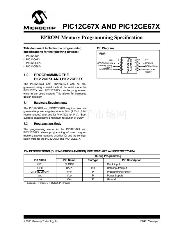
1.1
After receiving this command, the chip will load in a
14-bit 鈥渄ata word鈥?when 16 cycles are applied, as
described previously. A timing diagram for the load data
command is shown in Figure 4-1.
1.0.1.3
READ DATA
Programming Algorithm Requires
Variable V
DD
The PIC12C67X and PIC12CE67X uses an intelligent
algorithm. The algorithm calls for program veri铿乧ation
at V
DD
min as well as V
DD
max. Veri铿乧ation at V
DD
min
guarantees good 鈥渆rase margin鈥? Veri铿乧ation at
V
DD
max guarantees good 鈥減rogram margin鈥?
The actual programming must be done with V
DD
in the
V
DDP
range (4.75 - 5.25V).
V
DDP
= V
CC
range required during programming.
V
DD
min. = minimum operating V
DD
spec for the part.
V
DD
max.= maximum operating V
DD
spec for the part.
Programmers must verify the PIC12C67X and
PIC12CE67X at its speci铿乪d V
DD
max and V
DD
min lev-
els. Since Microchip may introduce future versions of
the PIC12C67X and PIC12CE67X with a broader V
DD
range, it is best that these levels are user selectable
(defaults are ok).
Note:
Any programmer not meeting these
requirements may only be classi铿乪d as
鈥減rototype鈥?or 鈥渄evelopment鈥?programmer
but not a 鈥減roduction鈥?quality programmer.
After receiving this command, the chip will transmit
data bits out of the memory currently accessed starting
with the second rising edge of the clock input. The GP0
pin will go into output mode on the second rising clock
edge, and it will revert back to input mode (hi-imped-
ance) after the 16th rising edge. A timing diagram of
this command is shown in Figure 4-2.
1.0.1.4
INCREMENT ADDRESS
The PC is incremented when this command is
received. A timing diagram of this command is shown
in Figure 4-3.
1.0.1.5
BEGIN PROGRAMMING
A load command (load con铿乬uration or load data)
must be given before every begin programming
command.
Programming of the appropriate memory
(test program memory or user program memory) will
begin after this command is received and decoded.
Programming should be performed with a series of
100
碌
s programming pulses. A programming pulse is
de铿乶ed as the time between the begin programming
command and the end programming command.
1.0.1.6
END PROGRAMMING
After receiving this command, the chip stops program-
ming the memory (con铿乬uration program memory or
user program memory) that it was programming at the
time.
漏
1998 Microchip Technology Inc.
DS40175A-page 7


 1
1
 2
2
 3
3
 4
4
 5
5
 6
6
 7
7
 8
8
 9
9
 10
10
 11
11
 12
12
 13
13
 14
14
