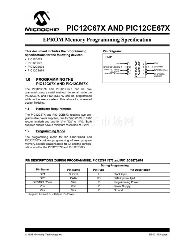
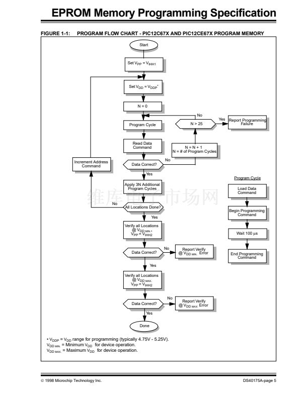
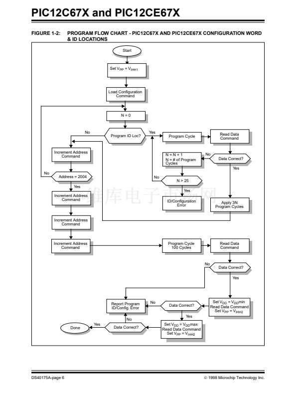
PIC12C67X and PIC12CE67X
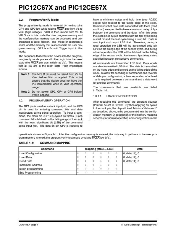
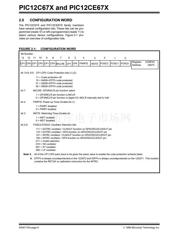
2.0
CONFIGURATION WORD
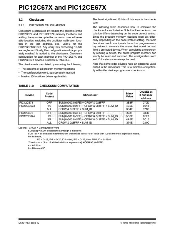
The PIC12C67X and PIC12CE67X family members
have several con铿乬uration bits. These bits can be pro-
grammed (reads '0') or left unprogrammed (reads '1') to
select various device con铿乬urations. Figure 2-1 pro-
vides an overview of con铿乬uration bits.
FIGURE 2-1:
Bit Number:
13
12
11
CONFIGURATION WORD
10
9
8
7
6
5
4
3
2
1
0
Register:
Address
CONFIG
2007h
CP1 CP0 CP1 CP0 CP1 CP0 MCLRE CP1 CP0 PWRTE
WDTE FOSC2 FOSC1 FOSC0
bit 13-8, 6-5: CP1:CP0: Code Protection bits (1) (2)
11 = Code protection off
10 = 0400h-07FFh code protected;
01 = 0200h-07FFh code protected;
00 = 0000h-07FFh code protected;
bit 7:
MCLRE: GP3/MCLR pin function select
1 = GP3/MCLR pin function is MCLR
0 = GP3/MCLR pin function is digital I/O, MCLR internally tied to Vdd
bit 4:
PWRTE: Power-up Timer Enable bit (1)
1 = PWRT disabled
0 = PWRT enabled
bit 3:
WDTE: Watchdog Timer Enable bit
1 = WDT enabled
0 = WDT disabled
bit 2-0:
FOSC2:FOSC0: Oscillator Selection bits
111 = EXTRC oscillator / CLKOUT function on GP4/OSC2/CLKOUT pin
110 = EXTRC oscillator / GP4 function on GP4/OSC2/CLKOUT pin
101 = INTRC oscillator / CLKOUT function on GP4/OSC2/CLKOUT pin
100 = INTRC oscillator / GP4 function on GP4/OSC2/CLKOUT pin
011 = invalid selection
010 = HS oscillator
001 = XT oscillator
000 = LP oscillator
Note 3:
All of the CP1:CP0 pairs have to be given the same value to enable the code protection scheme listed.
4:
07FFh is always uncodeprotected on the 12C672 and 03FFh is always uncodeprotected on the 12C671. This location
contains the RETLW xx calibration instruction for the INTRC.
DS40175A-page 8
漏
1998 Microchip Technology Inc.


 1
1
 2
2
 3
3
 4
4
 5
5
 6
6
 7
7
 8
8
 9
9
 10
10
 11
11
 12
12
 13
13
 14
14
