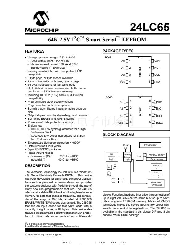
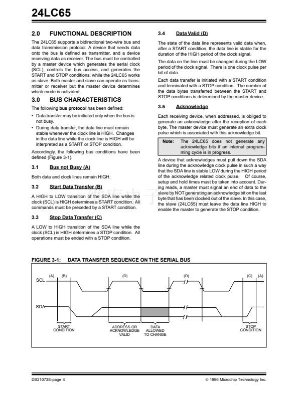
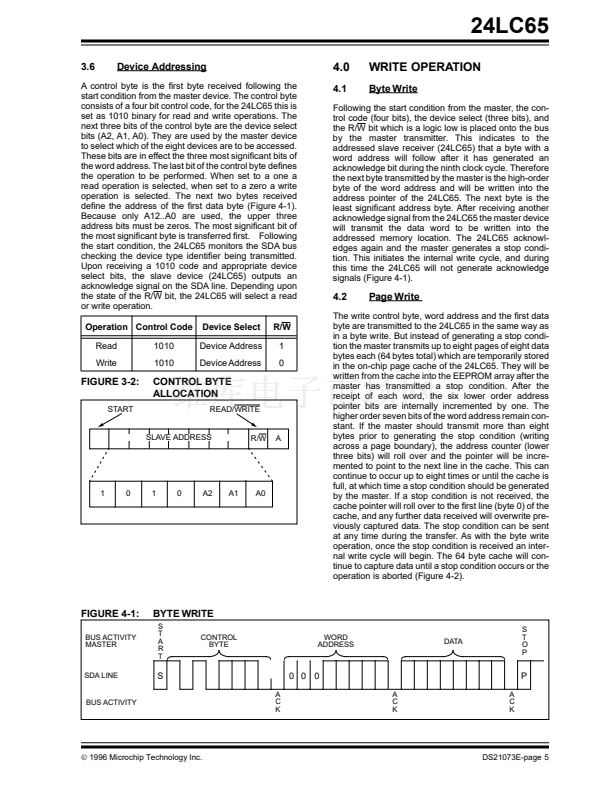
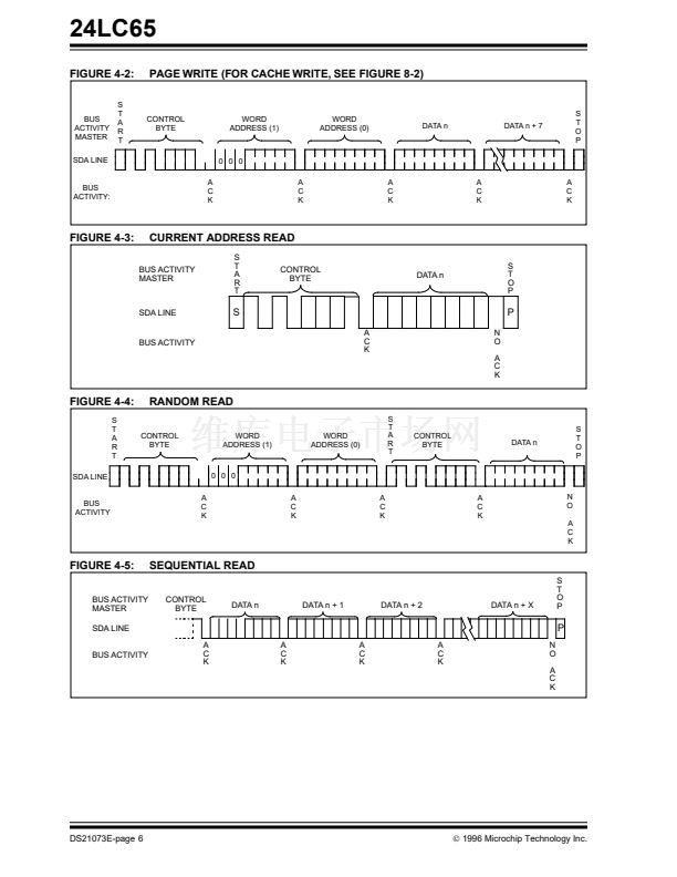
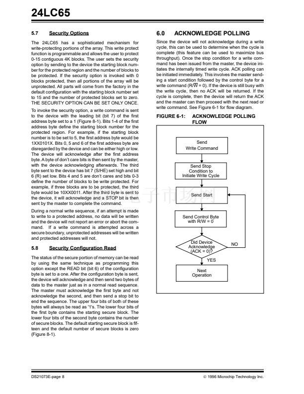
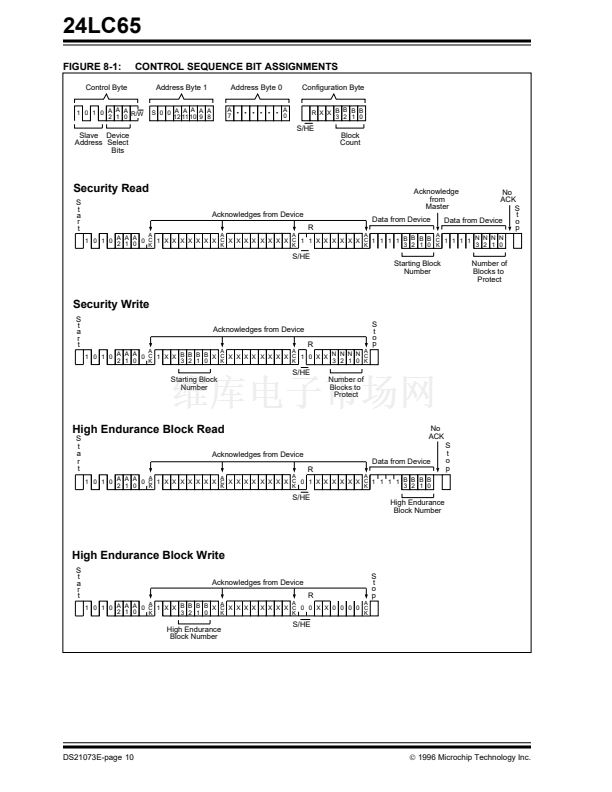
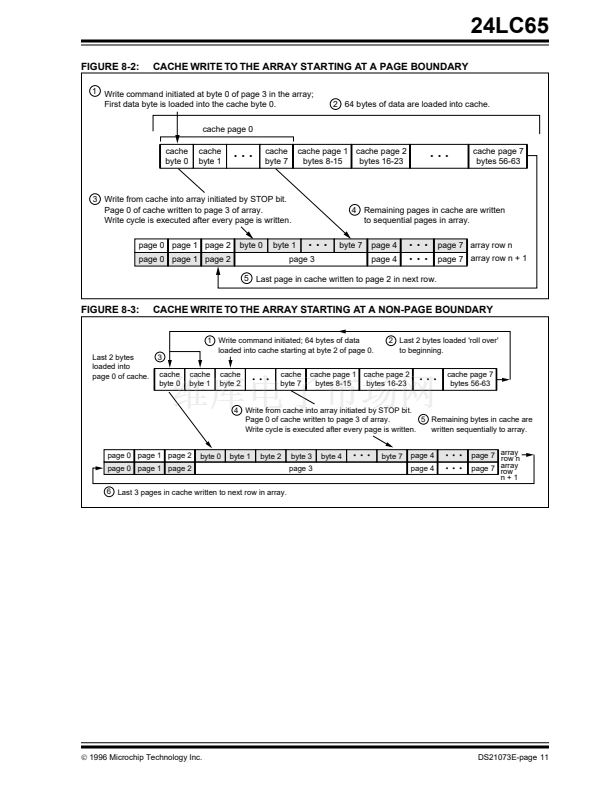
24LC65
5.0
READ OPERATION
5.4
Read operations are initiated in the same way as write
operations with the exception that the R/W bit of the
slave address is set to one. There are three basic types
of read operations: current address read, random read,
and sequential read.
Contiguous Addressing Across
Multiple Devices
5.1
Current Address Read
The device select bits A2, A1, A0 can be used to
expand the contiguous address space for up to 512K
bits by adding up to eight 24LC65's on the same bus. In
this case, software can use A0 of the control byte as
address bit A13, A1 as address bit A14, and A2 as
address bit A15.
The 24LC65 contains an address counter that main-
tains the address of the last word accessed, internally
incremented by one. Therefore, if the previous access
(either a read or write operation) was to address n (n is
any legal address), the next current address read oper-
ation would access data from address n + 1. Upon
receipt of the slave address with R/W bit set to one, the
24LC65 issues an acknowledge and transmits the eight
bit data word. The master will not acknowledge the
transfer but does generate a stop condition and the
24LC65 discontinues transmission (Figure 4-3).
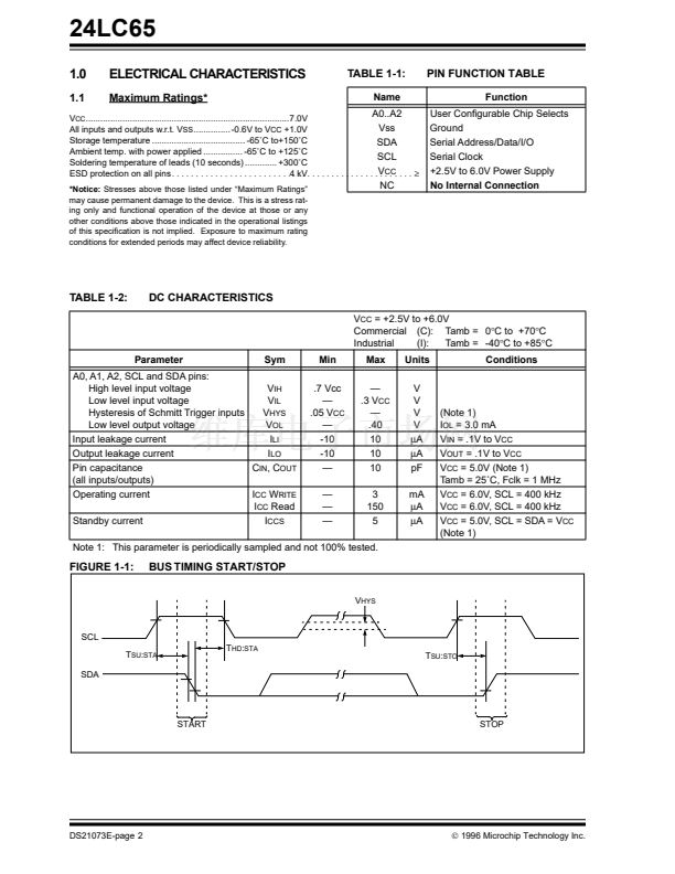
5.5
Noise Protection
The SCL and SDA inputs have 铿乴ter circuits which sup-
press noise spikes to assure proper device operation
even on a noisy bus. All I/O lines incorporate Schmitt
triggers for 400 KHz (Fast Mode) compatibility.
5.6
High Endurance Block
5.2
Random Read
Random read operations allow the master to access
any memory location in a random manner. To perform
this type of read operation, 铿乺st the word address must
be set. This is done by sending the word address to the
24LC65 as part of a write operation (R/W bit set to 0).
After the word address is sent, the master generates a
start condition following the acknowledge. This termi-
nates the write operation, but not before the internal
address pointer is set. Then the master issues the con-
trol byte again but with the R/W bit set to a one. The
24LC65 will then issue an acknowledge and transmit
the eight bit data word. The master will not acknowl-
edge the transfer but does generate a stop condition
which causes the 24LC65 to discontinue transmission
(Figure 4-4).
The location of the high-endurance block within the
memory map is programmed by setting the leading bit
7 (S/HE) of the con铿乬uration byte to 0. The upper bits
of the address loaded in this command will determine
which 4K block within the memory map will be set to
high endurance. This block will be capable of
10,000,000 ERASE/WRITE cycles typical (Figure 8-1).
Note:
The High Endurance Block cannot be
changed after the security option has been
set. If the H.E. block is not programmed by
the user, the default location is the highest
block of memory.
5.3
Sequential Read
Sequential reads are initiated in the same way as a ran-
dom read except that after the 24LC65 transmits the
铿乺st data byte, the master issues an acknowledge as
opposed to the stop condition used in a random read.
This acknowledge directs the 24LC65 to transmit the
next sequentially addressed 8 bit word (Figure 4-5).
Following the 铿乶al byte transmitted to the master, the
master will NOT generate an acknowledge but will gen-
erate a stop condition.
To provide sequential reads the 24LC65 contains an
internal address pointer which is incremented by one at
the completion of each operation. This address pointer
allows the entire memory contents to be serially read
during one operation.
漏
1996 Microchip Technology Inc.
DS21073E-page 7


 1
1
 2
2
 3
3
 4
4
 5
5
 6
6
 7
7
 8
8
 9
9
 10
10
 11
11
 12
12
