24LC65
7.0
PAGE CACHE AND ARRAY
MAPPING
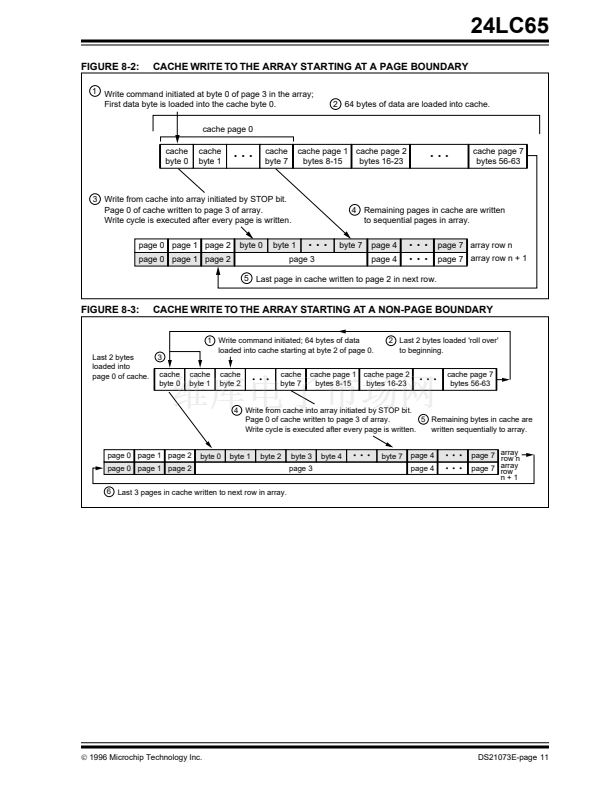
will 'roll over' and be loaded into the 铿乺st two bytes of
page 0 (of the cache). When the stop bit is sent, page
0 of the cache is written to page 3 of the array. The
remaining pages in the cache are then loaded sequen-
tially to the array. A write cycle is executed after each
page is written. If a partially loaded page in the cache
remains when the STOP bit is sent, only the bytes that
have been loaded will be written to the array.
The cache is a 64 byte (8 pages x 8 bytes) FIFO buffer.
The cache allows the loading of up to 64 bytes of data
before the write cycle is actually begun, effectively pro-
viding a 64-byte burst write at the maximum bus rate.
Whenever a write command is initiated, the cache
starts loading and will continue to load until a stop bit is
received to start the internal write cycle. The total length
of the write cycle will depend on how many pages are
loaded into the cache before the stop bit is given. Max-
imum cycle time for each page is 5 ms. Even if a page
is only partially loaded, it will still require the same cycle
time as a full page. If more than 64 bytes of data are
loaded before the stop bit is given, the address pointer
will 'wrap around' to the beginning of cache page 0 and
existing bytes in the cache will be overwritten. The
device will not respond to any commands while the
write cycle is in progress.
7.3
Power Management
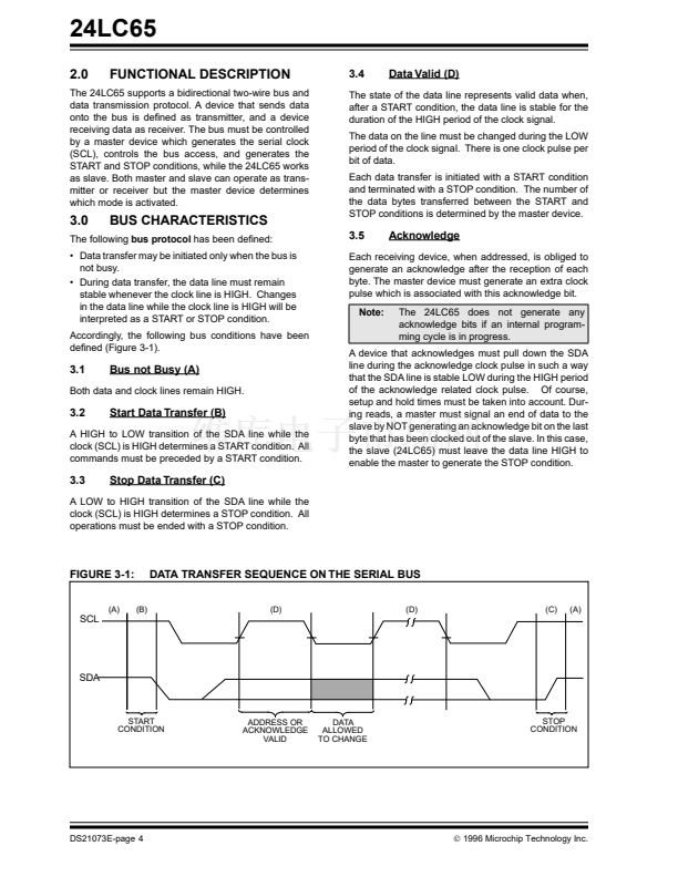
7.1
Cache Write Starting at a Page
Boundary
The design incorporates a power standby mode when
not in use and automatically powers off after the normal
termination of any operation when a stop bit is received
and all internal functions are complete. This includes
any error conditions, i.e. not receiving an acknowledge
or stop condition per the two-wire bus speci铿乧ation. The
device also incorporates V
DD
monitor circuitry to pre-
vent inadvertent writes (data corruption) during
low-voltage conditions. The V
DD
monitor circuitry is
powered off when the device is in standby mode in
order to further reduce power consumption.
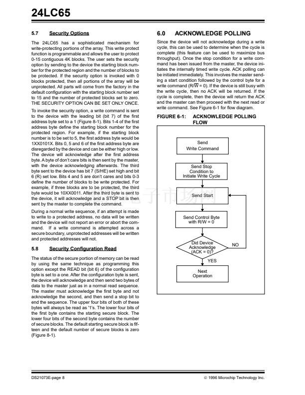
8.0
8.1
PIN DESCRIPTIONS
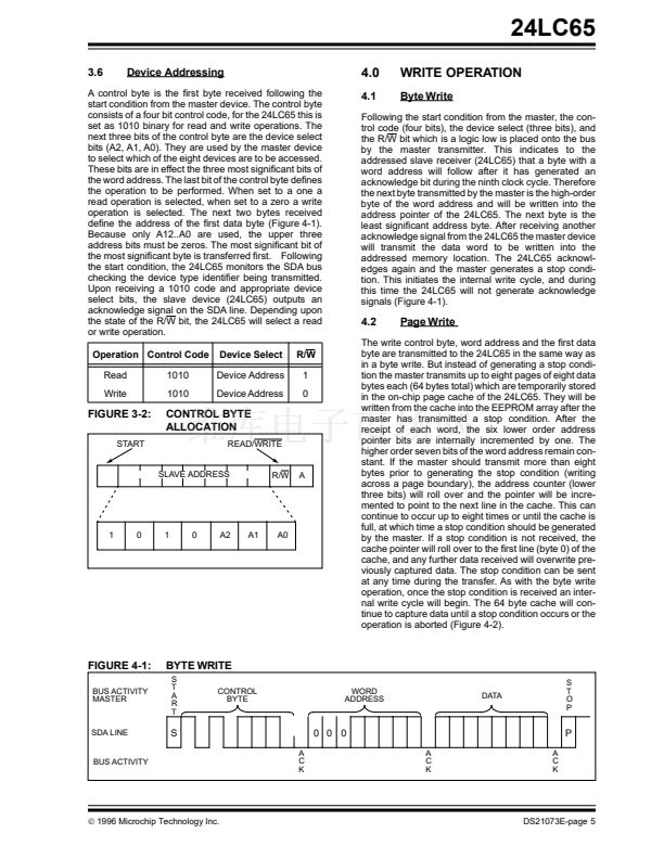
A0, A1, A2 Chip Address Inputs
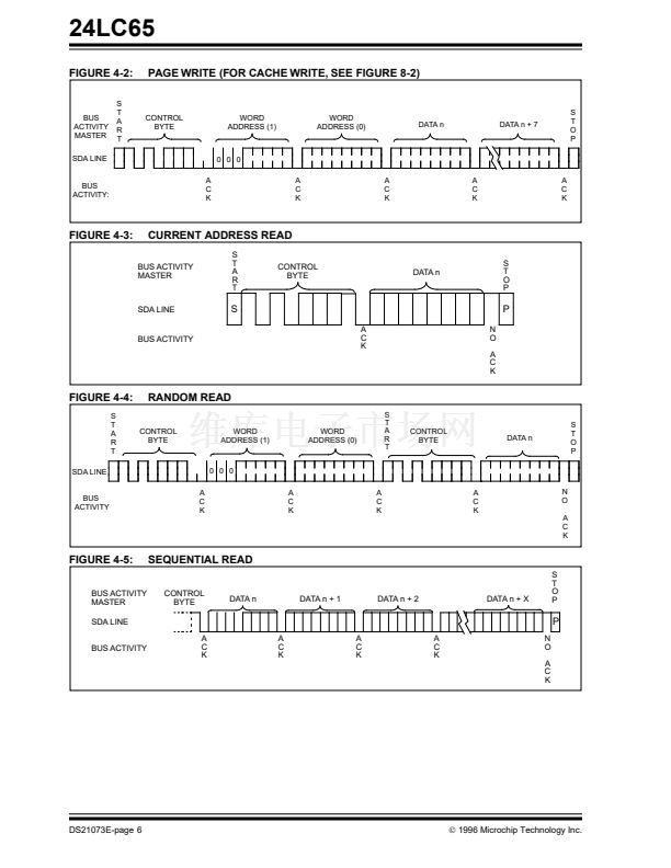
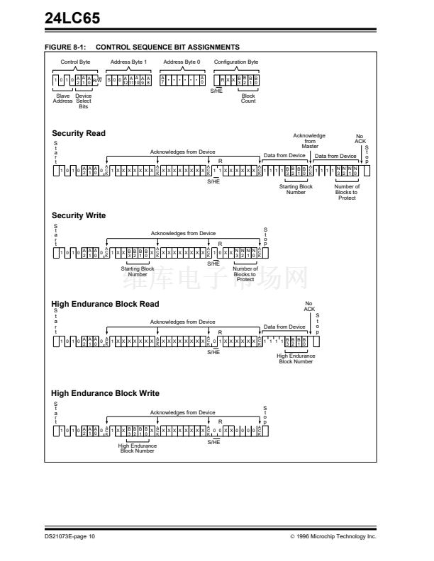
If a write command begins at a page boundary
(address bits A2, A1 and A0 are zero), then all data
loaded into the cache will be written to the array in
sequential addresses. This includes writing across a 4K
block boundary. In the example shown below,
(Figure 8-2) a write command is initiated starting at
byte 0 of page 3 with a fully loaded cache (64 bytes).
The 铿乺st byte in the cache is written to byte 0 of page 3
(of the array), with the remaining pages in the cache
written to sequential pages in the array. A write cycle is
executed after each page is written. Since the write
begins at page 3 and 8 pages are loaded into the
cache, the last 3 pages of the cache are written to the
next row in the array.
The A0..A2 inputs are used by the 24LC65 for multiple
device operation and conform to the two-wire bus stan-
dard. The levels applied to these pins de铿乶e the
address block occupied by the device in the address
map. A particular device is selected by transmitting the
corresponding bits (A2, A1, A0) in the control byte
(Figure 3-2 and Figure 8-1).
8.2
SDA Serial Address/Data Input/Output
7.2
Cache Write Starting at a Non-Page
Boundary
This is a bidirectional pin used to transfer addresses
and data into and data out of the device. It is an open
drain terminal, therefore the SDA bus requires a pullup
resistor to V
CC
(typical 10K鈩?for 100 kHz, 1K鈩?for 400
kHz).
For normal data transfer SDA is allowed to change only
during SCL low. Changes during SCL high are reserved
for indicating the START and STOP conditions.
When a write command is initiated that does not begin
at a page boundary (i.e., address bits A2, A1 and A0
are not all zero), it is important to note how the data is
loaded into the cache, and how the data in the cache is
written to the array. When a write command begins, the
铿乺st byte loaded into the cache is always loaded into
page 0. The byte within page 0 of the cache where the
load begins is determined by the three least signi铿乧ant
address bits (A2, A1, A0) that were sent as part of the
write command. If the write command does not start at
byte 0 of a page and the cache is fully loaded, then the
last byte(s) loaded into the cache will roll around to
page 0 of the cache and 铿乴l the remaining empty bytes.
If more than 64 bytes of data are loaded into the cache,
data already loaded will be overwritten. In the example
shown in Figure 8-3, a write command has been initi-
ated starting at byte 2 of page 3 in the array with a fully
loaded cache of 64 bytes. Since the cache started load-
ing at byte 2, the last two bytes loaded into the cache
8.3
SCL Serial Clock
This input is used to synchronize the data transfer from
and to the device.
漏
1996 Microchip Technology Inc.
DS21073E-page 9


 1
1
 2
2
 3
3
 4
4
 5
5
 6
6
 7
7
 8
8
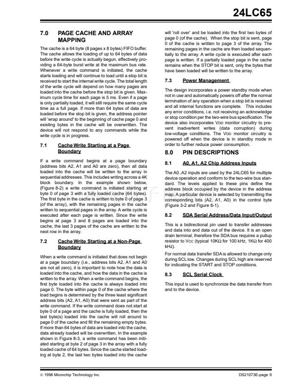 9
9
 10
10
 11
11
 12
12
