AD420
ABSOLUTE MAXIMUM RATINGS*
V
CC
23
V
CC
to GND
AD420AR/AN-32 . . . . . . . . . . . . . . . . . . . . . . . . . . . . . 32 V
I
OUT
to GND . . . . . . . . . . . . . . . . . . . . . . . . . . . . . . . . . . . V
CC
Digital Inputs to GND . . . . . . . . . . . . . . . . . . . 鈥?.5 V to +7 V
Digital Output to GND . . . . . . . . . . . . . 鈥?.5 V to V
LL
+ 0.3 V
V
LL
and REF OUT: Outputs Safe for Indefinite Short to Ground
Storage Temperature . . . . . . . . . . . . . . . . . . 鈥?5掳C to +150掳C
Lead Temperature (Soldering, 10 sec) . . . . . . . . . . . . +300掳C
Thermal Impedance:
SOIC (R) Package . . . . . . . . . . . . . . . . . . . . . .
胃
JA
= 75掳C/W
PDIP (N) Package . . . . . . . . . . . . . . . . . . . . . .
胃
JA
= 50掳C/W
*Stresses above those listed under Absolute Maximum Ratings may cause perma-
nent damage to the device. This is a stress rating only; functional operation of the
device at these or any other conditions above those indicated in the operational
section of this specification is not implied. Exposure to absolute maximum rating
conditions for extended periods may affect device reliability.
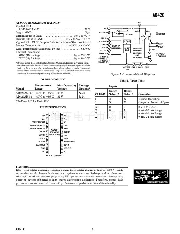
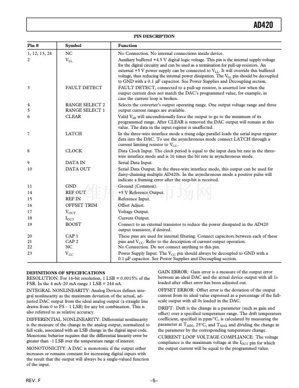
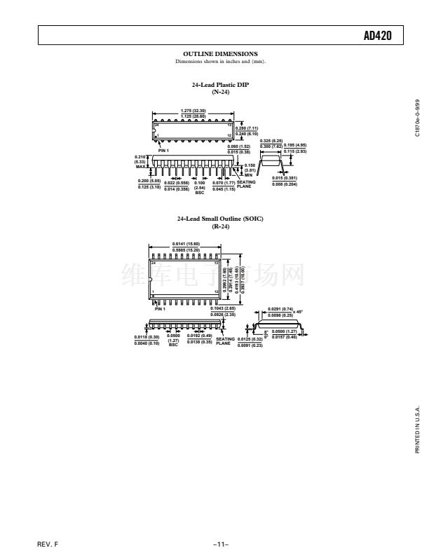
V
LL 2
REF OUT
14
REFERENCE
4k
40
19
BOOST
AD420
REF IN
15
DATA OUT
10
CLEAR
6
CLOCK
18
I
OUT
LATCH
7
CLOCK
8
DATA IN
9
DATA I/P
REGISTER
16-BIT
DAC
17
V
OUT
RANGE
5
SELECT 1
RANGE
4
SELECT 2
16
SWITCHED
CURRENT
SOURCES
AND
FILTERING
1.25k
3
FAULT
DETECT
20
21
11
OFFSET CAP 1 CAP 2 GND
TRIM
Figure 1. Functional Block Diagram
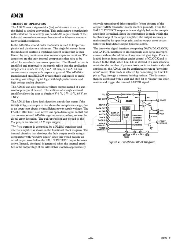
Table I. Truth Table
ORDERING GUIDE
Model
Temperature
Range
Max Operating Package
Voltage
Options*
32 V
32 V
N-24
R-24
CLEAR
0
1
X
X
X
X
Inputs
Range
Select 2
X
X
0
0
1
1
Range
Select 1
X
X
0
1
0
1
Operation
Normal Operation
Output at Bottom of Span
0 V鈥? V Range
4 mA鈥?0 mA Range
0 mA鈥?0 mA Range
0 mA鈥?4 mA Range
AD420AN-32 鈥?40掳C to +85掳C
AD420AR-32 鈥?40掳C to +85掳C
*N = Plastic DIP, R = Plastic SOIC.
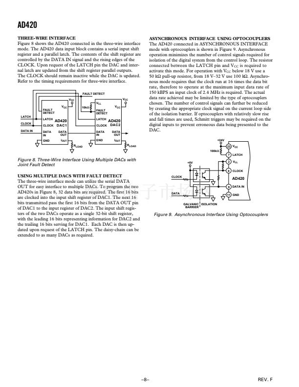
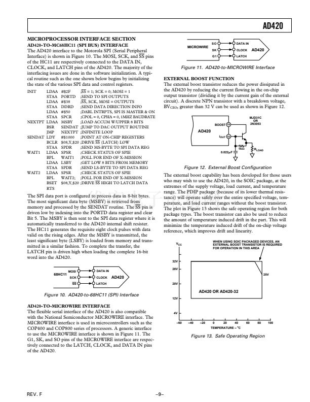
PIN DESIGNATIONS
NC
V
L L
FAULT DETECT
RANGE SELECT 2
RANGE SELECT 1
CLEAR
LATCH
CLOCK
DATA IN
DATA OUT
GND
NC
NC = NO CONNECT
NC
V
CC
NC
CAP2
AD420
TOP VIEW
(Not to Scale)
CAP1
BOOST
I
OUT
V
OUT
OFFSET TRIM
REF IN
REF OUT
NC
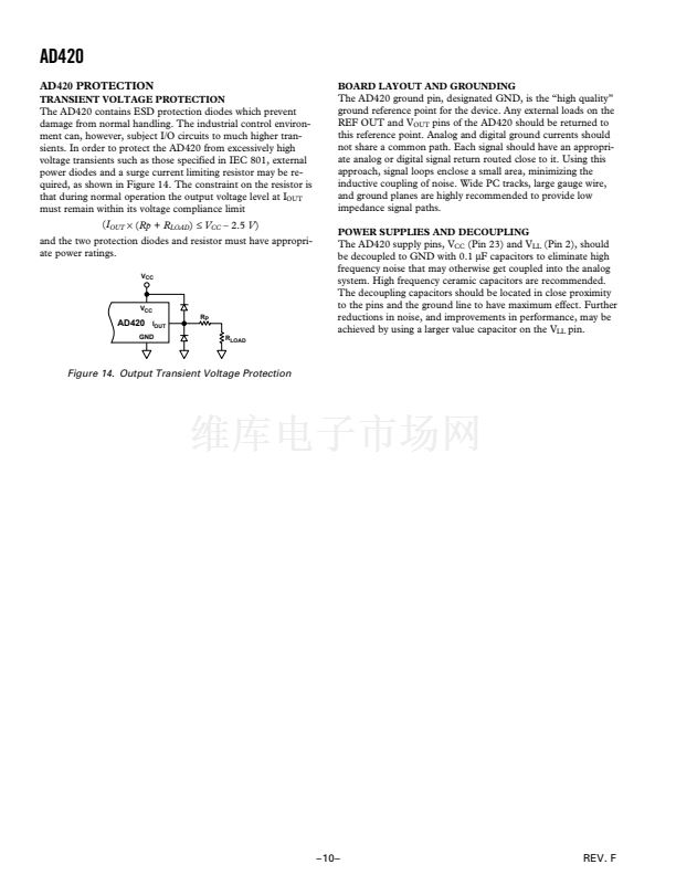
CAUTION
ESD (electrostatic discharge) sensitive device. Electrostatic charges as high as 4000 V readily
accumulate on the human body and test equipment and can discharge without detection.
Although the AD420 features proprietary ESD protection circuitry, permanent damage may
occur on devices subjected to high energy electrostatic discharges. Therefore, proper ESD
precautions are recommended to avoid performance degradation or loss of functionality.
WARNING!
ESD SENSITIVE DEVICE
REV. F
鈥?鈥?/div>
prev
next


 1
1
 2
2
 3
3
 4
4
 5
5
 6
6
 7
7
 8
8
 9
9
 10
10
 11
11
