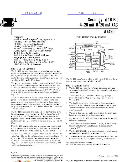
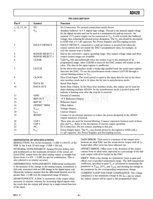
AD420
MICROPROCESSOR INTERFACE SECTION
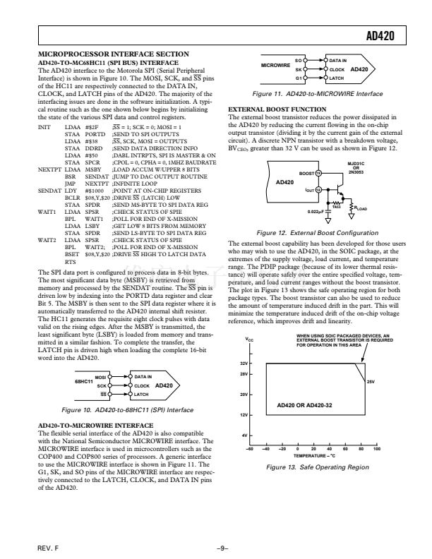
AD420-TO-MC68HC11 (SPI BUS) INTERFACE
SO
DATA IN
CLOCK
LATCH
The AD420 interface to the Motorola SPI (Serial Peripheral
Interface) is shown in Figure 10. The MOSI, SCK, and
SS
pins
of the HC11 are respectively connected to the DATA IN,
CLOCK, and LATCH pins of the AD420. The majority of the
interfacing issues are done in the software initialization. A typi-
cal routine such as the one shown below begins by initializing
the state of the various SPI data and control registers.
LDAA
STAA
LDAA
STAA
LDAA
STAA
NEXTPT LDAA
BSR
JMP
SENDAT LDY
BCLR
STAA
WAIT1
LDAA
BPL
LDAA
STAA
WAIT2
LDAA
BPL
BSET
RTS
INIT
#$2F
PORTD
#$38
DDRD
#$50
SPCR
MSBY
SENDAT
NEXTPT
#$1000
$08,Y,$20
SPDR
SPSR
WAIT1
LSBY
SPDR
SPSR
WAIT2;
$08,Y,$20
;SS = 1; SCK = 0; MOSI = 1
;SEND TO SPI OUTPUTS
;SS, SCK, MOSI = OUTPUTS
;SEND DATA DIRECTION INFO
;DABL INTRPTS, SPI IS MASTER & ON
;CPOL = 0, CPHA = 0, 1MHZ BAUDRATE
;LOAD ACCUM W/UPPER 8 BITS
;JUMP TO DAC OUTPUT ROUTINE
;INFINITE LOOP
;POINT AT ON-CHIP REGISTERS
;DRIVE
SS
(LATCH) LOW
;SEND MS-BYTE TO SPI DATA REG
;CHECK STATUS OF SPIE
;POLL FOR END OF X-MISSION
;GET LOW 8 BITS FROM MEMORY
;SEND LS-BYTE TO SPI DATA REG
;CHECK STATUS OF SPIE
;POLL FOR END OF X-MISSION
;DRIVE
SS
HIGH TO LATCH DATA
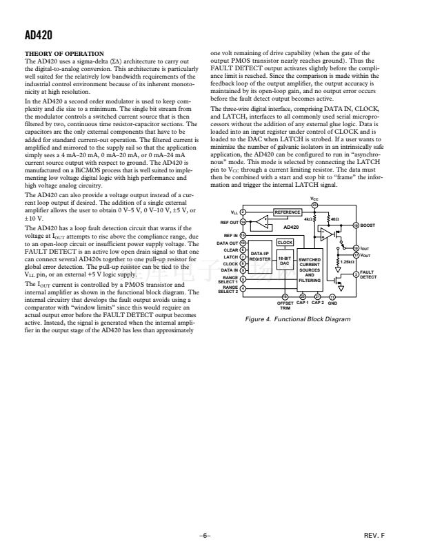
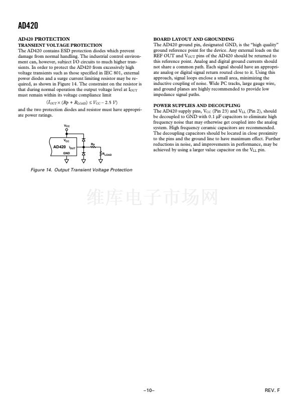
MICROWIRE
SK
G1
AD420
Figure 11. AD420-to-MICROWIRE Interface
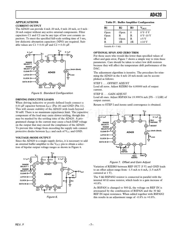
EXTERNAL BOOST FUNCTION
The external boost transistor reduces the power dissipated in
the AD420 by reducing the current flowing in the on-chip
output transistor (dividing it by the current gain of the external
circuit). A discrete NPN transistor with a breakdown voltage,
BV
CEO
, greater than 32 V can be used as shown in Figure 12.
MJD31C
OR
2N3053
BOOST
19
AD420
I
OUT 18
1k
0.022 F
R
LOAD
Figure 12. External Boost Configuration
The SPI data port is configured to process data in 8-bit bytes.
The most significant data byte (MSBY) is retrieved from
memory and processed by the SENDAT routine. The
SS
pin is
driven low by indexing into the PORTD data register and clear
Bit 5. The MSBY is then sent to the SPI data register where it is
automatically transferred to the AD420 internal shift resister.
The HC11 generates the requisite eight clock pulses with data
valid on the rising edges. After the MSBY is transmitted, the
least significant byte (LSBY) is loaded from memory and trans-
mitted in a similar fashion. To complete the transfer, the
LATCH pin is driven high when loading the complete 16-bit
word into the AD420.
MOSI
DATA IN
CLOCK
LATCH
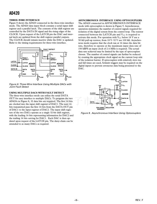
The external boost capability has been developed for those users
who may wish to use the AD420, in the SOIC package, at the
extremes of the supply voltage, load current, and temperature
range. The PDIP package (because of its lower thermal resis-
tance) will operate safely over the entire specified voltage, tem-
perature, and load current ranges without the boost transistor.
The plot in Figure 13 shows the safe operating region for both
package types. The boost transistor can also be used to reduce
the amount of temperature induced drift in the part. This will
minimize the temperature induced drift of the on-chip voltage
reference, which improves drift and linearity.
V
CC
WHEN USING SOIC PACKAGED DEVICES, AN
EXTERNAL BOOST TRANSISTOR IS REQUIRED
FOR OPERATION IN THIS AREA
32V
28V
68HC11
SCK
SS
AD420
20V
25V
Figure 10. AD420-to-68HC11 (SPI) Interface
12V
AD420 OR AD420-32
AD420-TO-MICROWIRE INTERFACE
The flexible serial interface of the AD420 is also compatible
with the National Semiconductor MICROWIRE interface. The
MICROWIRE interface is used in microcontrollers such as the
COP400 and COP800 series of processors. A generic interface
to use the MICROWIRE interface is shown in Figure 11. The
G1, SK, and SO pins of the MICROWIRE interface are respec-
tively connected to the LATCH, CLOCK, and DATA IN pins
of the AD420.
4V
鈥?0
鈥?0
鈥?0
0
20
40
60
80
100
TEMPERATURE 鈥?C
Figure 13. Safe Operating Region
REV. F
鈥?鈥?/div>
prev
next


 1
1
 2
2
 3
3
 4
4
 5
5
 6
6
 7
7
 8
8
 9
9
 10
10
 11
11
