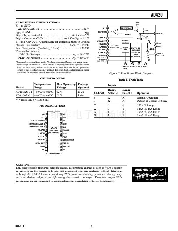
AD420
PIN DESCRIPTION
Pin #
1, 12, 13, 24
2
Symbol
NC
V
LL
Function
No Connection. No internal connections inside device.
Auxiliary buffered +4.5 V digital logic voltage. This pin is the internal supply voltage
for the digital circuitry and can be used as a termination for pull-up resistors. An
external +5 V power supply can be connected to V
LL
. It will override this buffered
voltage, thus reducing the internal power dissipation. The V
LL
pin should be decoupled
to GND with a 0.1
碌F
capacitor. See Power Supplies and Decoupling section.
FAULT DETECT, connected to a pull-up resistor, is asserted low when the
output current does not match the DAC鈥檚 programmed value, for example, in
case the current loop is broken.
Selects the converter鈥檚 output operating range. One output voltage range and three
output current ranges are available.
Valid V
IH
will unconditionally force the output to go to the minimum of its
programmed range. After CLEAR is removed the DAC output will remain at this
value. The data in the input register is unaffected.
In the three-wire interface mode a rising edge parallel loads the serial input register
data into the DAC. To use the asynchronous mode connect LATCH through a
current limiting resistor to V
CC
.
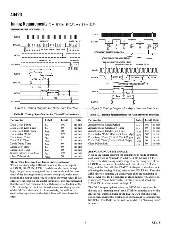
Data Clock Input. The clock period is equal to the input data bit rate in the three-
wire interface mode and is 16 times the bit rate in asynchronous mode.
Serial Data Input.
Serial Data Output. In the three-wire interface mode, this output can be used for
daisy-chaining multiple AD420s. In the asynchronous mode a positive pulse will
indicate a framing error after the stop-bit is received.
Ground (Common).
+5 V Reference Output.
Reference Input.
Offset Adjust.
Voltage Output.
Current Output.
Connect to an external transistor to reduce the power dissipated in the AD420
output transistor, if desired.
These pins are used for internal filtering. Connect capacitors between each of these
pins and V
CC
. Refer to the description of current output operation.
No Connection. Do not connect anything to this pin.
Power Supply Input. The V
CC
pin should always be decoupled to GND with a
0.1
碌F
capacitor. See Power Supplies and Decoupling section.
GAIN ERROR: Gain error is a measure of the output error
between an ideal DAC and the actual device output with all 1s
loaded after offset error has been adjusted out.
OFFSET ERROR: Offset error is the deviation of the output
current from its ideal value expressed as a percentage of the full-
scale output with all 0s loaded in the DAC.
DRIFT: Drift is the change in a parameter (such as gain and
offset) over a specified temperature range. The drift temperature
coefficient, specified in ppm/掳C, is calculated by measuring the
parameter at T
MIN
, 25掳C, and T
MAX
and dividing the change in
the parameter by the corresponding temperature change.
CURRENT LOOP VOLTAGE COMPLIANCE: The voltage
compliance is the maximum voltage at the I
OUT
pin for which
the output current will be equal to the programmed value.
3
FAULT DETECT
4
5
6
RANGE SELECT 2
RANGE SELECT 1
CLEAR
7
LATCH
8
9
10
CLOCK
DATA IN
DATA OUT
11
14
15
16
17
18
19
20
21
22
23
GND
REF OUT
REF IN
OFFSET TRIM
V
OUT
I
OUT
BOOST
CAP 1
CAP 2
NC
V
CC
DEFINITIONS OF SPECIFICATIONS
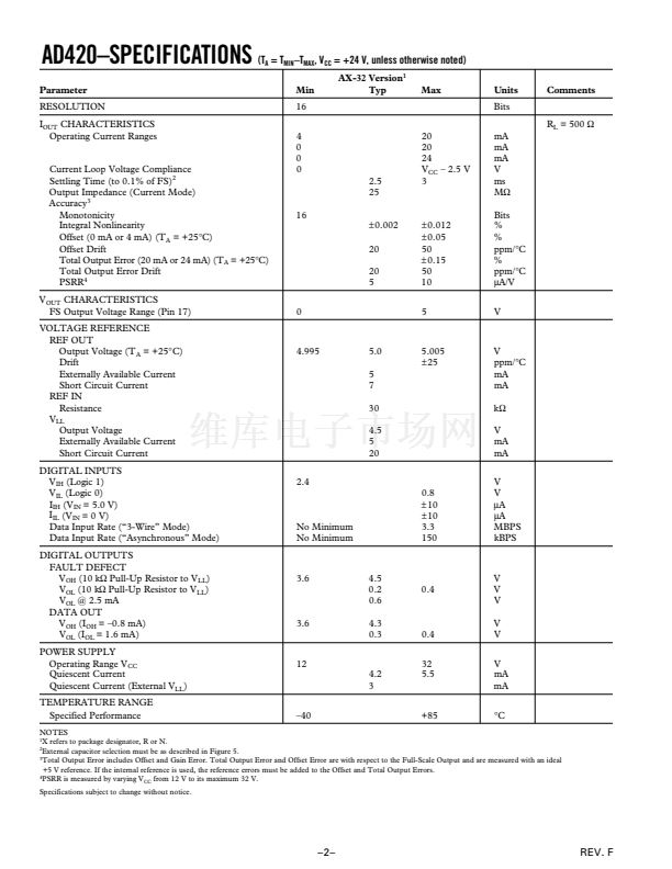
RESOLUTION: For 16-bit resolution, 1 LSB = 0.0015% of the
FSR. In the 4 mA鈥?0 mA range 1 LSB = 244 nA.
INTEGRAL NONLINEARITY: Analog Devices defines inte-
gral nonlinearity as the maximum deviation of the actual, ad-
justed DAC output from the ideal analog output (a straight line
drawn from 0 to FS 鈥?1 LSB) for any bit combination. This is
also referred to as relative accuracy.
DIFFERENTIAL NONLINEARITY: Differential nonlinearity
is the measure of the change in the analog output, normalized to
full scale, associated with an LSB change in the digital input code.
Monotonic behavior requires that the differential linearity error be
greater than 鈥? LSB over the temperature range of interest.
MONOTONICITY: A DAC is monotonic if the output either
increases or remains constant for increasing digital inputs with
the result that the output will always be a single-valued function
of the input.
REV. F
鈥?鈥?/div>
prev
next


 1
1
 2
2
 3
3
 4
4
 5
5
 6
6
 7
7
 8
8
 9
9
 10
10
 11
11
