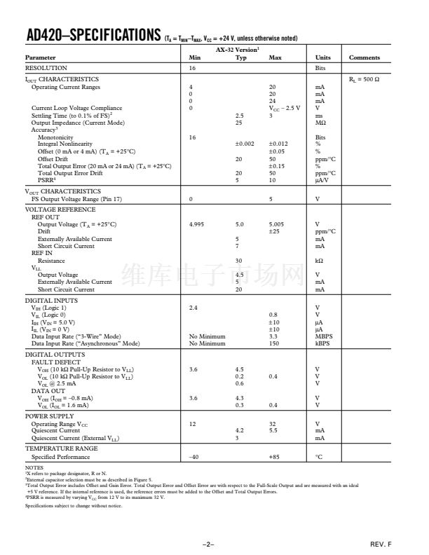
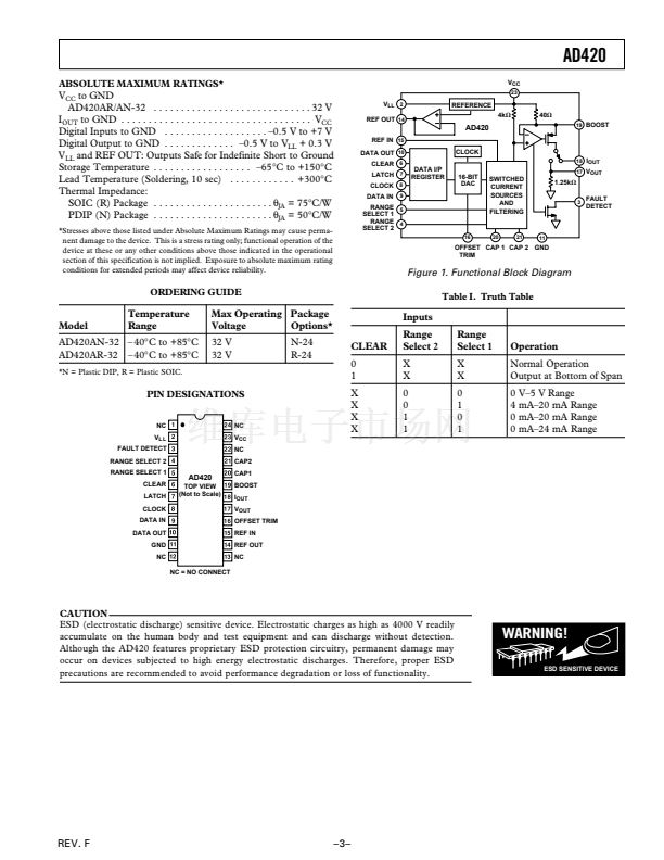
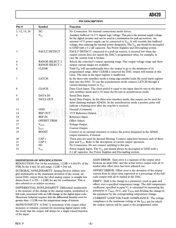
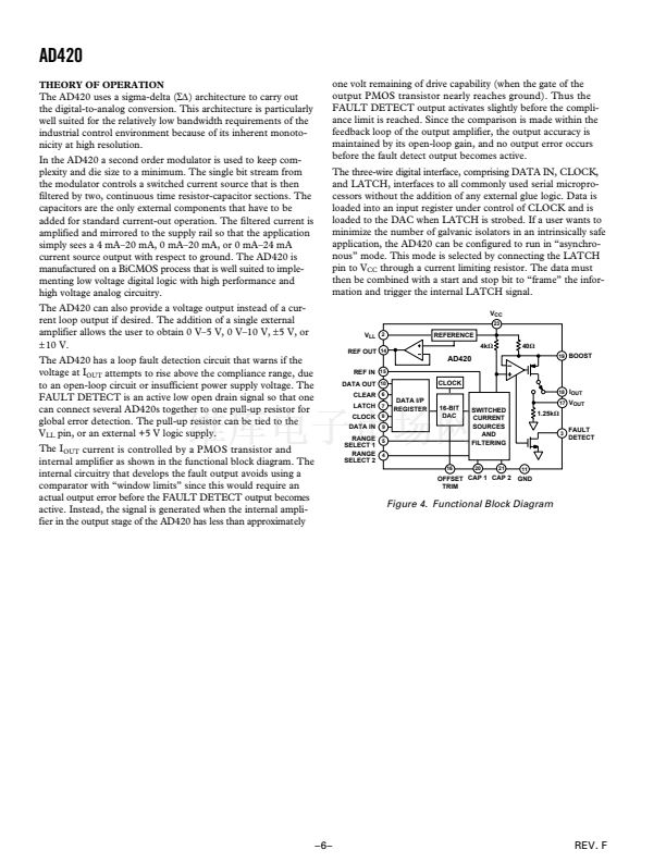
AD420
Timing Requirements
(T = 鈥?0 C to +85 C, V
A
CC
= +12 V to +32 V)
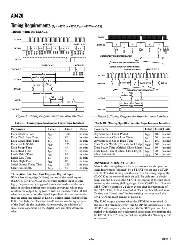
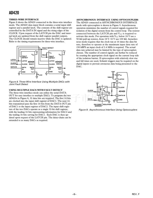
THREE-WIRE INTERFACE
CLOCK
CLOCK
WORD "N"
DATA IN
1 0
(MSB)
B15
B14
1 1
B13
B12
0 0
B11
B10
1
B9
0 0
B8
B7
111
B6
B5
B4
0 0
B3
B2
1 1
B1
B0
(LSB)
WORD "N + 1"
1
B15
0 0 1
B14
B13
B12
DATA IN
0
START
BIT
1
BIT 15
0
BIT 14
BITs
13-1
0
BIT 0
1
STOP
BIT
NEXT
START
BIT
(INTERNALLY GENERATED LATCH)
LATCH
EXPANDED TIME VIEW BELOW
WORD "N 鈥?1"
DATA OUT
WORD "N"
1 0
B15
B14
1 1
B13
B12
CLOCK
0 1
DATA IN
2
8
START BIT
16
24
DATA BIT 15
BIT 14
CLOCK COUNTER STARTS HERE
CONFIRM START BIT
SAMPLE BIT 15
t
CK
t
CL
CLOCK
t
CH
t
DS
t
DH
DATA IN
EXPANDED TIME VIEW BELOW
t
DW
t
LD
LATCH
t
ACK
t
ACL
t
LL
t
LH
t
SD
CLOCK
t
ADS
t
ADW
DATA IN
t
ACH
t
ADH
DATA OUT
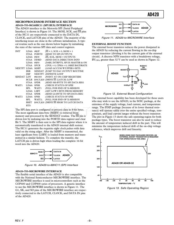
Figure 2. Timing Diagram for Three-Wire Interface
Table II. Timing Specification for Three-Wire Interface
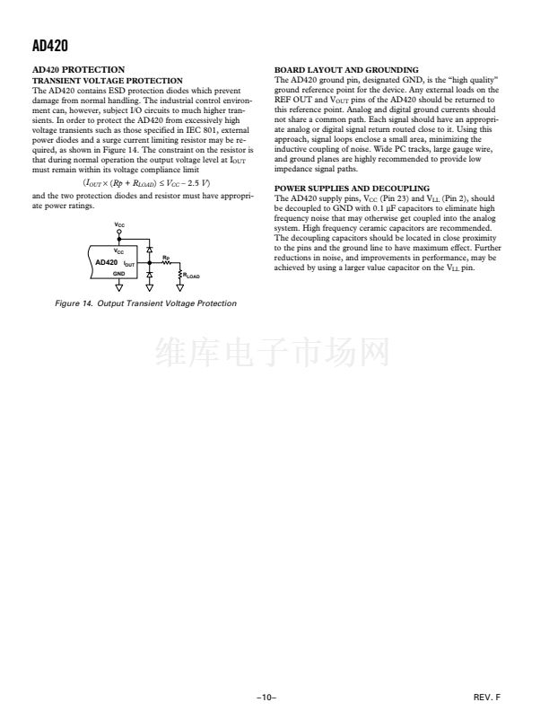
Figure 3. Timing Diagram for Asynchronous Interface
Table III. Timing Specifications for Asynchronous Interface
Parameter
Data Clock Period
Data Clock Low Time
Data Clock High Time
Data Stable Width
Data Setup Time
Data Hold Time
Latch Delay Time
Latch Low Time
Latch High Time
Serial Output Delay Time
Clear Pulsewidth
Label
t
CK
t
CL
t
CH
t
DW
t
DS
t
DH
t
LD
t
LL
t
LH
t
SD
t
CLR
Limit
300
80
80
125
40
5
80
80
80
225
50
Units
ns min
ns min
ns min
ns min
ns min
ns min
ns min
ns min
ns min
ns max
ns min
Parameter
Asynchronous Clock Period
Asynchronous Clock Low Time
Asynchronous Clock High Time
Data Stable Width (Critical Clock Edge)
Data Setup Time (Critical Clock Edge)
Data Hold Time (Critical Clock Edge)
Clear Pulsewidth
ASYNCHRONOUS INTERFACE
Label Limit Units
t
ACK
t
ACL
t
ACH
t
ADW
t
ADS
t
ADH
t
CLR
400
50
150
300
50
20
50
ns min
ns min
ns min
ns min
ns min
ns min
ns min
Three-Wire Interface Fast Edges on Digital Input
With a fast rising edge (<10 ns) on one of the serial inputs
(CLOCK, DATA IN, LATCH) while another input is logic
high, the part may be triggered into a test mode and the con-
tents of the data register may become corrupted, which may
result in the output being loaded with an incorrect value. If fast
edges are expected on the digital input lines, it is recommended
that the latch line remain at Logic 0 during serial loading of the
DAC. Similarly, the clock line should remain low during updates
of the DAC via the latch pin. Alternatively, the addition of
small value capacitors on the digital lines will slow down the
edge.
Note in the timing diagram for asynchronous mode operation
each data word is 鈥渇ramed鈥?by a START (0) bit and a STOP
(1) bit. The data timing is with respect to the rising edge of the
CLOCK at the center of each bit cell. Bit cells are 16 clocks
long, and the first cell (the START bit) begins at the first clock
following the leading (falling) edge of the START bit. Thus the
MSB (D15) is sampled 24 clock cycles after the beginning of
the START bit, D14 is sampled at clock number 40, and so on.
During any 鈥渄ead time鈥?before writing the next word the
DATA IN pin must remain at Logic 1.
The DAC output updates when the STOP bit is received. In
the case of a 鈥渇raming error鈥?(the STOP bit sampled as a 0) the
AD420 will output a pulse at the DATA OUT pin one clock
period wide during the clock period subsequent to sampling the
STOP bit. The DAC output will not update if a 鈥渇raming error鈥?/div>
is detected.
prev
next


 1
1
 2
2
 3
3
 4
4
 5
5
 6
6
 7
7
 8
8
 9
9
 10
10
 11
11
