AT24C64B
Pin Description
SERIAL CLOCK (SCL):
The SCL input is used to positive edge clock data into each
EEPROM device and negative edge clock data out of each device.
SERIAL DATA (SDA):
The SDA pin is bidirectional for serial data transfer. This pin is
open-drain driven and may be wire-ORed with any number of other open-drain or open
collector devices.
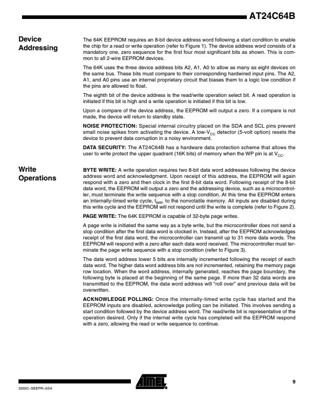
DEVICE/ADDRESSES (A2, A1, A0):
The A2, A1 and A0 pins are device address inputs
that are hard wired or left not connected for hardware compatibility with other AT24CXX
devices. When the pins are hardwired, as many as eight 64K devices may be addressed
on a single bus system (device addressing is discussed in detail under the Device
Addressing section). If the pins are left floating, the A2, A1 and A0 pins will be internally
pulled down to GND if the capacitive coupling to the circuit board V
CC
plane is <3pF.
If coupling is >3pF, Atmel recommends connecting the address pins to GND.
WRITE PROTECT (WP):
The write protect input, when connected to GND, allows nor-
mal write operations. When WP is connected high to V
CC
, all write operations to the
upper quandrant (16K bits) of memory are inhibited. If the pin is left floating, the WP pin
will be internally pulled down to GND if the capacitive coupling to the circuit board V
CC
plane is <3pF. If coupling is >3pF, Atmel recommends connecting the pin to GND.
Memory Organization
AT24C64B, 64K SERIAL EEPROM:
The 64K is internally organized as 256 pages of
32 bytes each. Random word addressing requires a 13 bit data word address.
3
3350C鈥揝EEPR鈥?/04


 1
1
 2
2
 3
3
 4
4
 5
5
 6
6
 7
7
 8
8
 9
9
 10
10
 11
11
 12
12
 13
13
 14
14
 15
15
 16
16
 17
17
