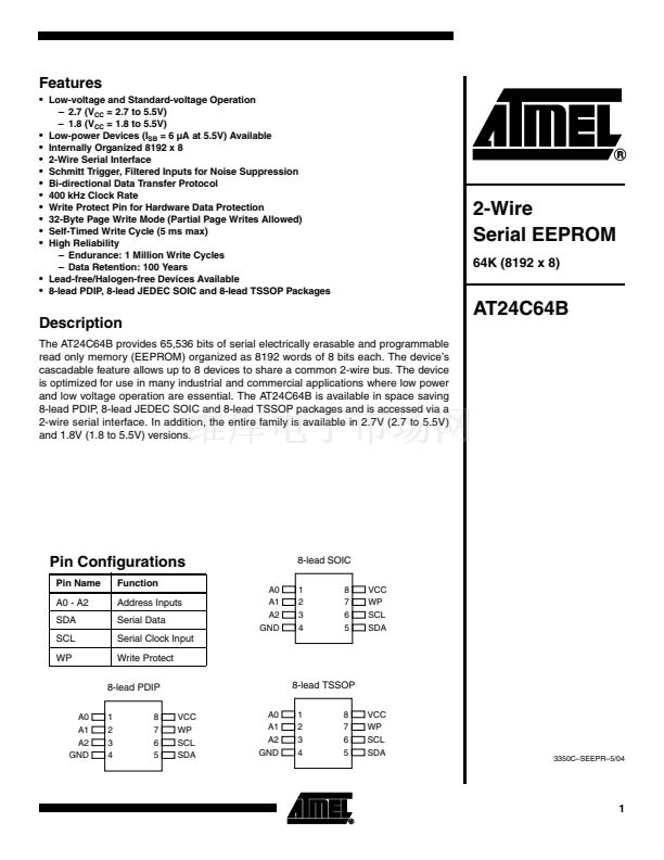
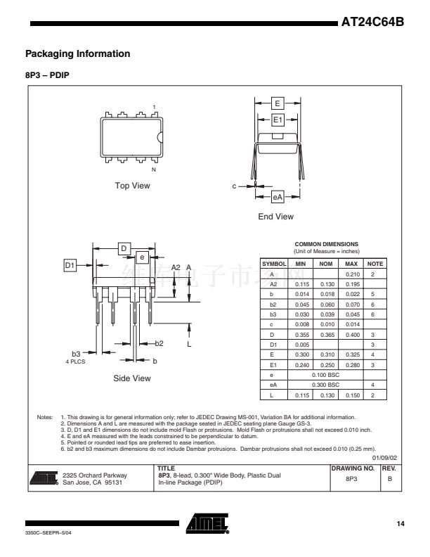
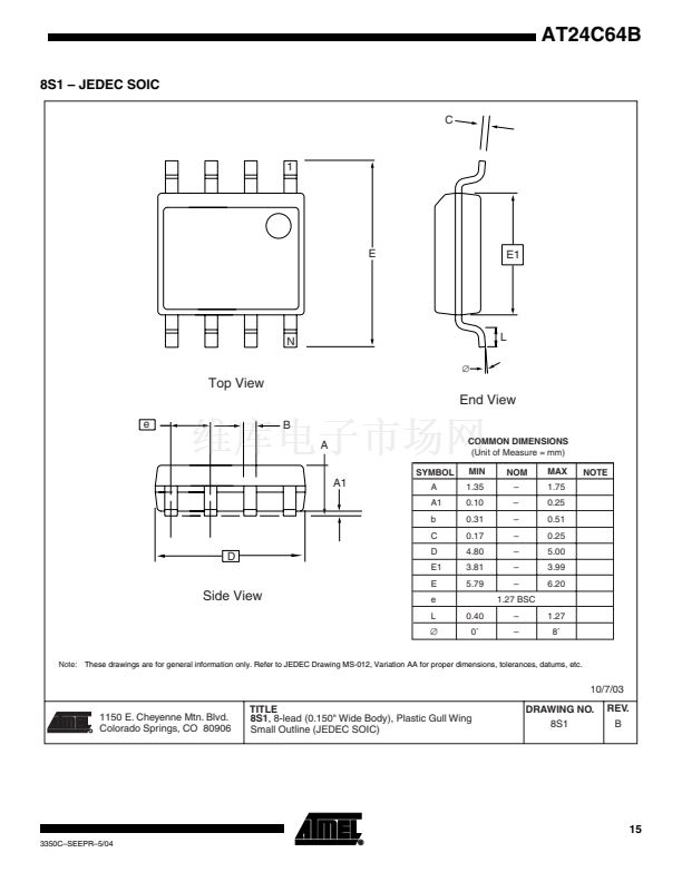
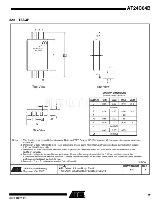
AT24C64B
Device
Addressing
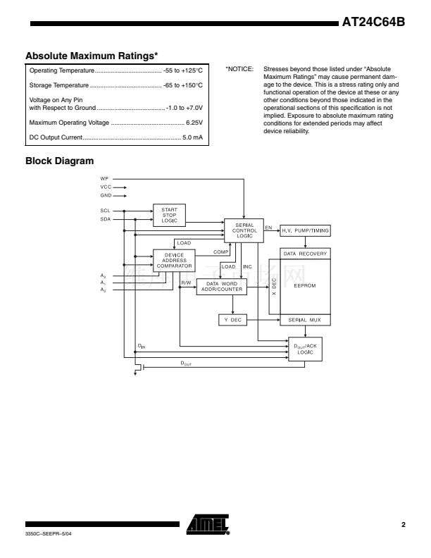
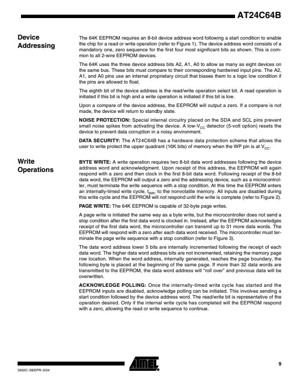
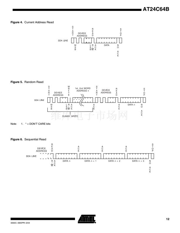
The 64K EEPROM requires an 8-bit device address word following a start condition to enable
the chip for a read or write operation (refer to Figure 1). The device address word consists of a
mandatory one, zero sequence for the first four most significant bits as shown. This is com-
mon to all 2-wire EEPROM devices.
The 64K uses the three device address bits A2, A1, A0 to allow as many as eight devices on
the same bus. These bits must compare to their corresponding hardwired input pins. The A2,
A1, and A0 pins use an internal proprietary circuit that biases them to a logic low condition if
the pins are allowed to float.
The eighth bit of the device address is the read/write operation select bit. A read operation is
initiated if this bit is high and a write operation is initiated if this bit is low.
Upon a compare of the device address, the EEPROM will output a zero. If a compare is not
made, the device will return to standby state.
NOISE PROTECTION:
Special internal circuitry placed on the SDA and SCL pins prevent
small noise spikes from activating the device. A low-V
CC
detector (5-volt option) resets the
device to prevent data corruption in a noisy environment.
DATA SECURITY:
The AT24C64B has a hardware data protection scheme that allows the
user to write protect the upper quadrant (16K bits) of memory when the WP pin is at V
CC
.
Write
Operations
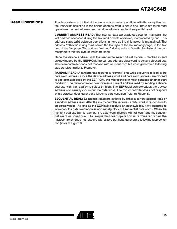
BYTE WRITE:
A write operation requires two 8-bit data word addresses following the device
address word and acknowledgment. Upon receipt of this address, the EEPROM will again
respond with a zero and then clock in the first 8-bit data word. Following receipt of the 8-bit
data word, the EEPROM will output a zero and the addressing device, such as a microcontrol-
ler, must terminate the write sequence with a stop condition. At this time the EEPROM enters
an internally-timed write cycle, t
WR
, to the nonvolatile memory. All inputs are disabled during
this write cycle and the EEPROM will not respond until the write is complete (refer to Figure 2).
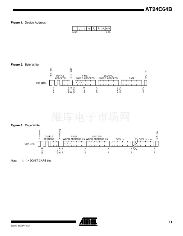
PAGE WRITE:
The 64K EEPROM is capable of 32-byte page writes.
A page write is initiated the same way as a byte write, but the microcontroller does not send a
stop condition after the first data word is clocked in. Instead, after the EEPROM acknowledges
receipt of the first data word, the microcontroller can transmit up to 31 more data words. The
EEPROM will respond with a zero after each data word received. The microcontroller must ter-
minate the page write sequence with a stop condition (refer to Figure 3).
The data word address lower 5 bits are internally incremented following the receipt of each
data word. The higher data word address bits are not incremented, retaining the memory page
row location. When the word address, internally generated, reaches the page boundary, the
following byte is placed at the beginning of the same page. If more than 32 data words are
transmitted to the EEPROM, the data word address will 鈥渞oll over鈥?and previous data will be
overwritten.
ACKNOWLEDGE POLLING:
Once the internally-timed write cycle has started and the
EEPROM inputs are disabled, acknowledge polling can be initiated. This involves sending a
start condition followed by the device address word. The read/write bit is representative of the
operation desired. Only if the internal write cycle has completed will the EEPROM respond
with a zero, allowing the read or write sequence to continue.
9
3350C鈥揝EEPR鈥?/04


 1
1
 2
2
 3
3
 4
4
 5
5
 6
6
 7
7
 8
8
 9
9
 10
10
 11
11
 12
12
 13
13
 14
14
 15
15
 16
16
 17
17
