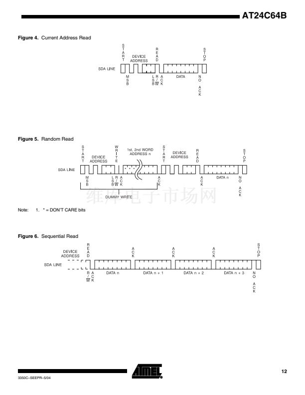
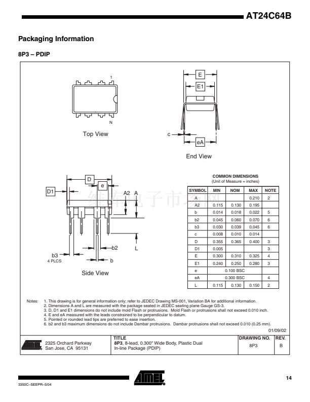
AT24C64B
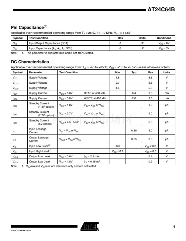
Pin Capacitance
(1)
Applicable over recommended operating range from T
A
= 25掳C, f = 1.0 MHz, V
CC
= +1.8V.
Symbol
C
I/O
C
IN
Note:
Test Condition
Input/Output Capacitance (SDA)
Input Capacitance (A
0
, A
1
, A
2
, SCL)
1. This parameter is characterized and is not 100% tested.
Max
8
6
Units
pF
pF
Conditions
V
I/O
= 0V
V
IN
= 0V
DC Characteristics
Applicable over recommended operating range from: T
AI
= -40 to +85掳C, V
CC
= +1.8 to +5.5V (unless otherwise noted).
Symbol
V
CC1
V
CC2
V
CC3
I
CC1
I
CC2
I
SB1
I
SB2
I
SB3
I
LI
I
LO
V
IL
V
IH
V
OL2
V
OL1
Note:
Parameter
Supply Voltage
Supply Voltage
Supply Voltage
Supply Current
Supply Current
Standby Current
(1.8V option)
Standby Current
(2.7V option)
Standby Current
(5V option)
Input Leakage
Current
Output Leakage
Current
Input Low Level
(1)
Input High Level
(1)
Output Low Level
Output Low Level
V
CC
= 3.0V
V
CC
= 1.8V
I
OL
= 2.1 mA
I
OL
= 0.15 mA
V
CC
= 5.0V
V
CC
= 5.0V
V
CC
= 1.8V
V
CC
= 2.7V
V
CC
= 4.5 - 5.5V
V
IN
= V
CC
or V
SS
V
OUT
= V
CC
or V
SS
-0.6
V
CC
x 0.7
READ at 400 kHz
WRITE at 400 kHz
V
IN
= V
CC
or V
SS
V
IN
= V
CC
or V
SS
V
IN
= V
CC
or V
SS
0.10
0.05
Test Condition
Min
1.8
2.7
4.5
0.4
2.0
Typ
Max
5.5
5.5
5.5
1.0
3.0
1.0
2.0
6.0
3.0
3.0
V
CC
x 0.3
V
CC
+ 0.5
0.4
0.2
Units
V
V
V
mA
mA
碌A
碌A
碌A
碌A
碌A
V
V
V
V
1. V
IL
min and V
IH
max are reference only and are not tested.
4
3350C鈥揝EEPR鈥?/04


 1
1
 2
2
 3
3
 4
4
 5
5
 6
6
 7
7
 8
8
 9
9
 10
10
 11
11
 12
12
 13
13
 14
14
 15
15
 16
16
 17
17
